


Share

8T49N240-035NLGI8
Manufacturer No:
8T49N240-035NLGI8
Manufacturer:
Description:
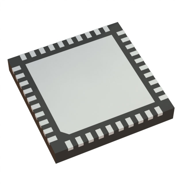
IC JITTER ATTEN 40VFQFPN
Datasheet:
Delivery:


Payment:


In Stock : 0
Please send RFQ , we will respond immediately.


8T49N240-035NLGI8 Specifications
-
TypeParameter
-
Supplier Device Package40-VFQFPN (6x6)
-
Package / Case40-VFQFN Exposed Pad
-
Mounting TypeSurface Mount
-
Operating Temperature-40°C ~ 85°C (TA)
-
Voltage - Supply2.375V ~ 2.625V, 3.135V ~ 3.465V
-
Divider/MultiplierYes/No
-
Frequency - Max867MHz
-
Differential - Input:OutputYes/Yes
-
Ratio - Input:Output2:4
-
Number of Circuits1
-
OutputHCSL, LVCMOS, LVDS, LVPECL
-
InputLVCMOS, LVDS, LVHSTL, LVPECL, Crystal
-
PLLYes
-
TypeJitter Attenuator
-
DigiKey ProgrammableNot Verified
-
PackagingTape & Reel (TR)
-
Product StatusActive
-
SeriesFemtoClock® NG
The SI5341A-B04366-GM is a highly integrated clock generator and jitter attenuator chip manufactured by Silicon Labs. It offers several advantages and can be applied in various scenarios. Some of the advantages and application scenarios of the SI5341A-B04366-GM are:Advantages: 1. High Integration: The chip integrates multiple clock generation and distribution functions into a single device, reducing the need for additional components and simplifying the overall system design. 2. Low Jitter: It provides excellent jitter performance, ensuring accurate and reliable clock signals for various applications. 3. Flexible Configuration: The chip offers extensive programmability options, allowing users to configure and customize the clock outputs according to their specific requirements. 4. Multiple Clock Outputs: It supports up to 12 differential clock outputs, enabling the distribution of multiple clock signals to different components or subsystems. 5. Low Power Consumption: The chip is designed to operate with low power consumption, making it suitable for power-sensitive applications.Application Scenarios: 1. Telecommunications: The SI5341A-B04366-GM can be used in telecommunications equipment, such as routers, switches, and base stations, to generate and distribute clock signals for synchronization and timing purposes. 2. Data Centers: It can be employed in data center infrastructure, including servers, storage systems, and network switches, to provide accurate clock signals for data transmission and processing. 3. Test and Measurement: The chip is suitable for test and measurement equipment, where precise timing and synchronization are crucial for accurate measurements and data acquisition. 4. Broadcast and Video Equipment: It can be utilized in broadcast and video equipment, such as cameras, video routers, and production switchers, to generate synchronized clock signals for video processing and distribution. 5. Industrial Automation: The chip can find applications in industrial automation systems, providing accurate timing signals for synchronized operation of various components and devices.These are just a few examples of the advantages and application scenarios of the SI5341A-B04366-GM chip. Its versatility, programmability, and high-performance characteristics make it suitable for a wide range of applications requiring precise clock generation and distribution.
8T49N240-035NLGI8 Relevant information
-

SI5332BD11784-GM2R
Skyworks Solutions Inc. -
SI5332BD12441-GM2R
Skyworks Solutions Inc. -
SI5332BD13549-GM2R
Skyworks Solutions Inc. -
SI5332BD11107-GM2R
Skyworks Solutions Inc. -
SI5332BD11650-GM2R
Skyworks Solutions Inc. -
SI5332BD13507-GM2R
Skyworks Solutions Inc. -
SI5332BD11320-GM2R
Skyworks Solutions Inc. -
SI5332BD13696-GM2R
Skyworks Solutions Inc. -
SI5332BD13619-GM2R
Skyworks Solutions Inc. -
SI5332BD11748-GM2R
Skyworks Solutions Inc.