


Share

CDCVF857DGG
Manufacturer No:
CDCVF857DGG
Manufacturer:
Description:
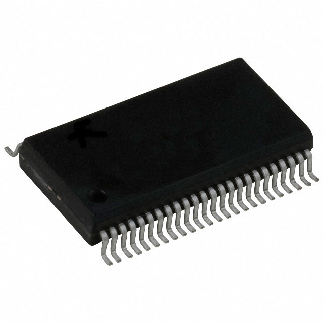
IC PLL CLOCK DRIVER 48TSSOP
Datasheet:
Delivery:


Payment:


In Stock : 0
Please send RFQ , we will respond immediately.


CDCVF857DGG Specifications
-
TypeParameter
-
Supplier Device Package48-TSSOP
-
Package / Case48-TFSOP (0.240", 6.10mm Width)
-
Mounting TypeSurface Mount
-
Operating Temperature-40°C ~ 85°C
-
Voltage - Supply2.3V ~ 2.7V
-
Divider/MultiplierNo/No
-
Frequency - Max220MHz
-
Differential - Input:OutputYes/Yes
-
Ratio - Input:Output2:11
-
Number of Circuits1
-
OutputSSTL-2
-
InputSSTL-2
-
PLLYes with Bypass
-
TypePLL Clock Driver
-
DigiKey ProgrammableNot Verified
-
PackagingTube
-
PackagingBulk
-
Product StatusActive
-
Series-
The CDCVF857DGG is an integrated circuit chip that belongs to the family of voltage level translators. It is specifically designed for translating signals between different voltage domains. Here are some advantages and application scenarios of the CDCVF857DGG:Advantages: 1. Voltage Level Translation: The primary advantage of the CDCVF857DGG is its ability to translate signals between different voltage domains. It supports translation between 3.3V and 5V logic levels, making it suitable for interfacing between different microcontrollers, sensors, and other digital devices.2. Bidirectional Translation: The CDCVF857DGG supports bidirectional voltage level translation, allowing signals to be translated in both directions. This flexibility makes it suitable for applications where data needs to be transmitted in both directions between different voltage domains.3. High-Speed Operation: The CDCVF857DGG is designed to operate at high speeds, making it suitable for applications that require fast data transmission. It supports data rates up to 200 Mbps, enabling it to handle high-speed communication protocols like I2C, SPI, UART, etc.4. Low Power Consumption: The CDCVF857DGG is designed to operate with low power consumption, making it suitable for battery-powered devices or applications where power efficiency is crucial.Application Scenarios: 1. Interfacing Microcontrollers: The CDCVF857DGG can be used to interface microcontrollers operating at different voltage levels. For example, it can be used to connect a 3.3V microcontroller to a 5V peripheral device, allowing them to communicate seamlessly.2. Sensor Interfaces: Many sensors operate at different voltage levels than the microcontroller or controller they are connected to. The CDCVF857DGG can be used to translate the voltage levels between the sensor and the controller, enabling data exchange.3. Communication Buses: The CDCVF857DGG can be used in various communication buses like I2C, SPI, UART, etc., to enable communication between devices operating at different voltage levels. It ensures compatibility and reliable data transfer between devices.4. Mixed Voltage Systems: In systems where different components operate at different voltage levels, the CDCVF857DGG can be used to bridge the voltage gaps and enable seamless communication and data transfer.Overall, the CDCVF857DGG is a versatile voltage level translator chip that finds applications in various scenarios where voltage level translation is required for reliable and efficient data communication.
CDCVF857DGG Relevant information
-
SI5332BD11784-GM2R
Skyworks Solutions Inc. -
SI5332BD12441-GM2R
Skyworks Solutions Inc. -
SI5332BD13549-GM2R
Skyworks Solutions Inc. -
SI5332BD11107-GM2R
Skyworks Solutions Inc. -
SI5332BD11650-GM2R
Skyworks Solutions Inc. -
SI5332BD13507-GM2R
Skyworks Solutions Inc. -
SI5332BD11320-GM2R
Skyworks Solutions Inc. -
SI5332BD13696-GM2R
Skyworks Solutions Inc. -
SI5332BD13619-GM2R
Skyworks Solutions Inc. -
SI5332BD11748-GM2R
Skyworks Solutions Inc.