


Share
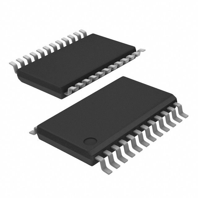

CDCVF2509PWR
Manufacturer No:
CDCVF2509PWR
Manufacturer:
Description:
IC PLL CLOCK DRIVER 24TSSOP
Datasheet:
Delivery:


Payment:


In Stock : 0
Please send RFQ , we will respond immediately.


CDCVF2509PWR Specifications
-
TypeParameter
-
Operating Temperature0°C ~ 85°C
-
Voltage - Supply3V ~ 3.6V
-
Divider/MultiplierNo/No
-
Frequency - Max175MHz
-
Differential - Input:OutputNo/No
-
Ratio - Input:Output2:10
-
Number of Circuits1
-
OutputLVTTL
-
InputLVTTL
-
PLLYes with Bypass
-
TypePLL Clock Driver
-
Supplier Device Package24-TSSOP
-
Package / Case24-TSSOP (0.173", 4.40mm Width)
-
Mounting TypeSurface Mount
-
DigiKey ProgrammableNot Verified
-
PackagingCut Tape (CT)
-
PackagingTape & Reel (TR)
-
Product StatusActive
-
Series-
The CDCVF2509PWR is a high-performance clock driver integrated circuit chip manufactured by Texas Instruments. It offers several advantages and can be applied in various scenarios. Some of the advantages and application scenarios of the CDCVF2509PWR are:Advantages: 1. High-performance Clock Distribution: The CDCVF2509PWR is designed to distribute high-frequency clock signals with minimal skew and jitter, ensuring accurate and synchronized timing across multiple components or subsystems. 2. Low Output Skew: It provides low output skew, which means that the clock signals reach their destination at nearly the same time, reducing timing errors and improving system performance. 3. Wide Operating Frequency Range: The chip supports a wide range of operating frequencies, making it suitable for various applications requiring different clock speeds. 4. Low Power Consumption: The CDCVF2509PWR is designed to operate with low power consumption, making it suitable for battery-powered devices or applications where power efficiency is crucial. 5. Small Form Factor: The chip comes in a small form factor package, making it suitable for space-constrained applications or designs where board space is limited.Application Scenarios: 1. High-Speed Data Communication: The CDCVF2509PWR can be used in high-speed data communication systems, such as Ethernet switches, routers, or optical transceivers, to distribute clock signals accurately and synchronize data transmission. 2. Memory Interfaces: It can be used in memory modules, such as DDR (Double Data Rate) or SDRAM (Synchronous Dynamic Random Access Memory), to distribute clock signals and ensure synchronized data transfer between the memory and the controller. 3. FPGA/ASIC Clock Distribution: The chip can be used in FPGA (Field-Programmable Gate Array) or ASIC (Application-Specific Integrated Circuit) designs to distribute clock signals to various components, ensuring proper synchronization and timing. 4. Test and Measurement Equipment: The CDCVF2509PWR can be used in test and measurement equipment, such as oscilloscopes or logic analyzers, to distribute clock signals accurately and synchronize measurements across multiple channels. 5. Industrial Automation: It can be used in industrial automation systems, such as programmable logic controllers (PLCs) or motion control systems, to distribute clock signals and synchronize various components for precise timing and control.These are just a few examples of the advantages and application scenarios of the CDCVF2509PWR integrated circuit chip. Its versatility, high-performance clock distribution capabilities, and low power consumption make it suitable for a wide range of applications requiring accurate timing and synchronization.
CDCVF2509PWR Relevant information
-
SI5332BD11784-GM2R
Skyworks Solutions Inc. -
SI5332BD12441-GM2R
Skyworks Solutions Inc. -
SI5332BD13549-GM2R
Skyworks Solutions Inc. -
SI5332BD11107-GM2R
Skyworks Solutions Inc. -
SI5332BD11650-GM2R
Skyworks Solutions Inc. -
SI5332BD13507-GM2R
Skyworks Solutions Inc. -
SI5332BD11320-GM2R
Skyworks Solutions Inc. -
SI5332BD13696-GM2R
Skyworks Solutions Inc. -
SI5332BD13619-GM2R
Skyworks Solutions Inc. -
SI5332BD11748-GM2R
Skyworks Solutions Inc.