


Share
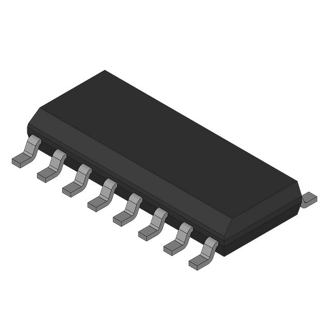

CY23S08ZXC-1H
Manufacturer No:
CY23S08ZXC-1H
Manufacturer:
Description:
IC FANOUT BUFFER 16TSSOP
Datasheet:
Delivery:


Payment:


In Stock : 10500
Please send RFQ , we will respond immediately.


CY23S08ZXC-1H Specifications
-
TypeParameter
-
Supplier Device Package16-TSSOP
-
Package / Case16-TSSOP (0.173", 4.40mm Width)
-
Mounting TypeSurface Mount
-
Operating Temperature0°C ~ 70°C
-
Voltage - Supply3V ~ 3.6V
-
Divider/MultiplierNo/No
-
Frequency - Max140MHz
-
Differential - Input:OutputNo/No
-
Ratio - Input:Output1:8
-
Number of Circuits1
-
OutputLVCMOS
-
InputLVCMOS, LVTTL
-
PLLYes with Bypass
-
TypeFanout Buffer (Distribution), Zero Delay Buffer
-
DigiKey ProgrammableNot Verified
-
PackagingTube
-
Product StatusObsolete
-
Series-
The SI5345A-D06985-GM is a highly flexible and programmable clock generator and jitter attenuator integrated circuit (IC) chip. It offers several advantages and can be used in various application scenarios, including:1. High Flexibility: The SI5345A-D06985-GM chip provides a wide range of frequency synthesis and clock distribution options. It can generate up to 12 different output clocks with different frequencies, phases, and formats, making it suitable for complex clocking requirements.2. Low Jitter: The IC chip incorporates advanced jitter attenuation techniques, which help in reducing the noise and jitter in the generated clocks. This makes it ideal for applications that require precise and stable clock signals, such as high-speed data communication, networking, and test and measurement equipment.3. Programmability: The chip is highly programmable, allowing users to configure various parameters such as output frequencies, input references, and clock formats. This flexibility enables customization and adaptation to different system requirements, making it suitable for a wide range of applications.4. Multiple Input References: The SI5345A-D06985-GM chip supports multiple input references, including crystal oscillators, LVCMOS, LVDS, and differential PECL inputs. This versatility allows it to interface with different types of clock sources, making it compatible with various system architectures.5. Low Power Consumption: The IC chip is designed to operate with low power consumption, making it suitable for power-sensitive applications such as portable devices, battery-powered equipment, and energy-efficient systems.Application scenarios for the SI5345A-D06985-GM chip include:1. Telecommunications: The chip can be used in telecommunications equipment, such as routers, switches, and base stations, to generate and distribute precise clock signals for data synchronization and timing.2. Data Centers: In data centers, the chip can be used for clocking applications in servers, storage systems, and network switches, ensuring accurate timing and synchronization for high-speed data transmission.3. Test and Measurement: The IC chip can be utilized in test and measurement equipment, such as oscilloscopes, signal generators, and spectrum analyzers, to generate stable and precise clock signals for accurate measurements and analysis.4. Broadcast and Video Equipment: The chip can be employed in broadcast and video equipment, including cameras, video routers, and production switchers, to provide synchronized clock signals for video processing and distribution.5. Industrial Automation: The chip can be used in industrial automation systems, such as programmable logic controllers (PLCs) and motion control systems, to generate accurate clock signals for synchronization and timing of various processes.Overall, the SI5345A-D06985-GM chip offers high flexibility, low jitter, and programmability, making it suitable for a wide range of applications that require precise and stable clock signals.
CY23S08ZXC-1H Relevant information
-
SI5332BD11784-GM2R
Skyworks Solutions Inc. -
SI5332BD12441-GM2R
Skyworks Solutions Inc. -
SI5332BD13549-GM2R
Skyworks Solutions Inc. -
SI5332BD11107-GM2R
Skyworks Solutions Inc. -
SI5332BD11650-GM2R
Skyworks Solutions Inc. -
SI5332BD13507-GM2R
Skyworks Solutions Inc. -
SI5332BD11320-GM2R
Skyworks Solutions Inc. -
SI5332BD13696-GM2R
Skyworks Solutions Inc. -
SI5332BD13619-GM2R
Skyworks Solutions Inc. -
SI5332BD11748-GM2R
Skyworks Solutions Inc.