


Share

CDCM7005ZVAR
Manufacturer No:
CDCM7005ZVAR
Manufacturer:
Description:
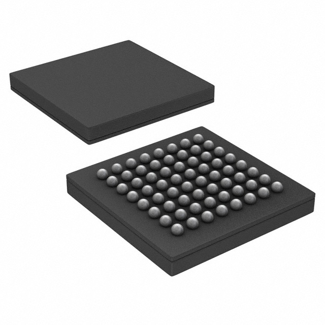
IC CLOCK SYNCHRONIZER 64BGA
Datasheet:
Delivery:


Payment:


In Stock : 0
Please send RFQ , we will respond immediately.


CDCM7005ZVAR Specifications
-
TypeParameter
-
Supplier Device Package64-BGA (8x8)
-
Package / Case64-LFBGA
-
Mounting TypeSurface Mount
-
Operating Temperature-40°C ~ 85°C
-
Voltage - Supply3V ~ 3.6V
-
Divider/MultiplierYes/No
-
Frequency - Max1.5GHz
-
Differential - Input:OutputYes/Yes
-
Ratio - Input:Output3:10
-
Number of Circuits1
-
OutputLVCMOS, LVPECL
-
InputLVCMOS, LVPECL
-
PLLYes with Bypass
-
TypeClock Synchronizer and Jitter Cleaner
-
DigiKey ProgrammableNot Verified
-
PackagingTape & Reel (TR)
-
Product StatusActive
-
Series-
The CDCM7005ZVAR is a high-performance clock generator and jitter cleaner integrated circuit chip. It offers several advantages and can be applied in various scenarios:1. Low jitter: The CDCM7005ZVAR chip provides low jitter clock signals, which is crucial in applications where timing accuracy is essential, such as high-speed data communication, networking, and digital signal processing.2. Multiple outputs: It offers up to 10 differential clock outputs, making it suitable for applications that require multiple synchronized clocks, such as high-speed data converters, FPGA/ASIC clock distribution, and multi-channel communication systems.3. Flexible frequency synthesis: The chip supports frequency synthesis from a wide range of input references, allowing it to generate clock signals at various frequencies. This flexibility makes it suitable for applications that require different clock frequencies, such as telecommunications, wireless communication, and multimedia systems.4. Jitter cleaning: The CDCM7005ZVAR chip includes a jitter cleaner circuit that can reduce the phase noise and jitter of the input reference clock. This feature is beneficial in scenarios where the input clock signal is noisy or has excessive jitter, ensuring a clean and stable clock signal for downstream components.5. Programmability: The chip offers programmable features, such as output dividers, phase-locked loop (PLL) settings, and clock skew adjustment. This programmability allows customization and optimization of the clock signals for specific application requirements.Application scenarios for the CDCM7005ZVAR chip include:1. Data communication: It can be used in high-speed data communication systems, such as Ethernet switches, routers, and optical transceivers, to generate synchronized clock signals for data transmission and reception.2. Networking: The chip can be employed in network switches, routers, and servers to provide accurate clock signals for data processing, packet forwarding, and synchronization between network devices.3. Digital signal processing: It is suitable for applications that involve digital signal processing, such as software-defined radios, base stations, and radar systems, where precise clock synchronization is crucial for accurate signal processing and data conversion.4. Test and measurement: The CDCM7005ZVAR chip can be utilized in test and measurement equipment, such as oscilloscopes, logic analyzers, and signal generators, to generate stable and synchronized clock signals for accurate measurements and signal analysis.5. Broadcast and multimedia: It can be used in broadcast equipment, video/audio processing systems, and multimedia devices to generate synchronized clock signals for video/audio encoding, decoding, and synchronization.Overall, the CDCM7005ZVAR chip's advantages of low jitter, multiple outputs, flexible frequency synthesis, jitter cleaning, and programmability make it suitable for a wide range of applications requiring high-performance clock generation and synchronization.
CDCM7005ZVAR Relevant information
-
SI5332BD11784-GM2R
Skyworks Solutions Inc. -
SI5332BD12441-GM2R
Skyworks Solutions Inc. -
SI5332BD13549-GM2R
Skyworks Solutions Inc. -
SI5332BD11107-GM2R
Skyworks Solutions Inc. -
SI5332BD11650-GM2R
Skyworks Solutions Inc. -
SI5332BD13507-GM2R
Skyworks Solutions Inc. -
SI5332BD11320-GM2R
Skyworks Solutions Inc. -
SI5332BD13696-GM2R
Skyworks Solutions Inc. -
SI5332BD13619-GM2R
Skyworks Solutions Inc. -
SI5332BD11748-GM2R
Skyworks Solutions Inc.