


Share
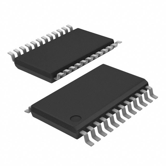

CDC2510BPWR
Manufacturer No:
CDC2510BPWR
Manufacturer:
Description:
IC PLL CLOCK DRIVER 24TSSOP
Datasheet:
Delivery:


Payment:


In Stock : 0
Please send RFQ , we will respond immediately.


CDC2510BPWR Specifications
-
TypeParameter
-
Supplier Device Package24-TSSOP
-
Package / Case24-TSSOP (0.173", 4.40mm Width)
-
Mounting TypeSurface Mount
-
Operating Temperature0°C ~ 70°C
-
Voltage - Supply3V ~ 3.6V
-
Divider/MultiplierNo/No
-
Frequency - Max125MHz
-
Differential - Input:OutputNo/No
-
Ratio - Input:Output1:10
-
Number of Circuits1
-
OutputClock
-
InputClock
-
PLLYes with Bypass
-
TypePLL Clock Driver
-
DigiKey ProgrammableNot Verified
-
PackagingCut Tape (CT)
-
PackagingTape & Reel (TR)
-
Product StatusNot For New Designs
-
Series-
The CDC2510BPWR is a specific integrated circuit chip manufactured by Texas Instruments. It is a high-performance clock driver and fanout buffer designed for clock distribution applications. Some of the advantages and application scenarios of the CDC2510BPWR chip are:1. High-performance clock distribution: The CDC2510BPWR chip is specifically designed for clock distribution applications, providing high-performance clock buffering and fanout capabilities. It can distribute clock signals with minimal skew and jitter, ensuring accurate and synchronized timing across multiple devices.2. Low output skew and jitter: The chip offers low output skew and jitter, which is crucial for applications that require precise timing synchronization. It helps in maintaining signal integrity and reducing timing errors in high-speed digital systems.3. Wide operating frequency range: The CDC2510BPWR chip supports a wide operating frequency range, typically from a few megahertz to several gigahertz. This makes it suitable for various clock distribution applications, including telecommunications, networking, data centers, and high-speed digital designs.4. Multiple output options: The chip provides multiple output options, including differential and single-ended outputs. This flexibility allows it to interface with different types of devices and clocking architectures, making it versatile for various application scenarios.5. Small form factor and low power consumption: The CDC2510BPWR chip comes in a small form factor and consumes low power, making it suitable for space-constrained designs and energy-efficient applications.6. Clock distribution in FPGA and ASIC designs: The chip can be used for clock distribution in field-programmable gate array (FPGA) and application-specific integrated circuit (ASIC) designs. It helps in distributing clock signals to different components within the FPGA or ASIC, ensuring proper synchronization and timing.7. High-speed data communication: The CDC2510BPWR chip can be used in high-speed data communication systems, such as Ethernet switches, routers, and optical networking equipment. It helps in distributing clock signals to various data processing and transmission components, ensuring reliable and synchronized data transfer.Overall, the CDC2510BPWR integrated circuit chip offers high-performance clock distribution capabilities, low skew and jitter, wide frequency range, and multiple output options. It finds applications in various industries, including telecommunications, networking, data centers, FPGA/ASIC designs, and high-speed data communication systems.
CDC2510BPWR Relevant information
-
SI5332BD11784-GM2R
Skyworks Solutions Inc. -
SI5332BD12441-GM2R
Skyworks Solutions Inc. -
SI5332BD13549-GM2R
Skyworks Solutions Inc. -
SI5332BD11107-GM2R
Skyworks Solutions Inc. -
SI5332BD11650-GM2R
Skyworks Solutions Inc. -
SI5332BD13507-GM2R
Skyworks Solutions Inc. -
SI5332BD11320-GM2R
Skyworks Solutions Inc. -
SI5332BD13696-GM2R
Skyworks Solutions Inc. -
SI5332BD13619-GM2R
Skyworks Solutions Inc. -
SI5332BD11748-GM2R
Skyworks Solutions Inc.