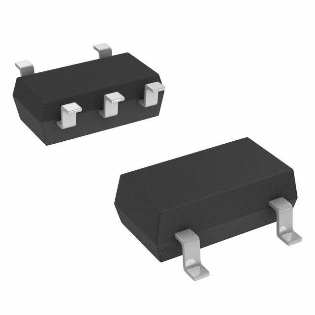
In Stock : 18381
Please send RFQ , we will respond immediately.


FXLP34P5X Specifications
-
TypeParameter
-
Supplier Device PackageSC-70-5
-
Package / Case5-TSSOP, SC-70-5, SOT-353
-
Mounting TypeSurface Mount
-
Features-
-
Operating Temperature-40°C ~ 85°C (TA)
-
Data Rate-
-
Output TypeNon-Inverted
-
Output Signal-
-
Input Signal-
-
Voltage - VCCB1 V ~ 3.6 V
-
Voltage - VCCA1 V ~ 3.6 V
-
Channels per Circuit1
-
Number of Circuits1
-
Channel TypeUnidirectional
-
Translator TypeVoltage Level
-
PackagingCut Tape (CT)
-
PackagingTape & Reel (TR)
-
Product StatusActive
-
Series-
The CD4504BD3 integrated circuit chip is a hex buffer and converter that can be used in various applications. Here are some advantages and application scenarios of this chip:Advantages: 1. High-speed operation: The CD4504BD3 chip operates at high speeds, allowing for efficient data transfer and processing. 2. Low power consumption: It is designed to consume minimal power, making it suitable for battery-operated devices and power-sensitive applications. 3. Wide supply voltage range: The chip supports a wide range of supply voltages (3V to 15V), providing flexibility in different power supply scenarios. 4. Hex buffer and converter: The CD4504BD3 chip contains six buffer stages, enabling it to convert and amplify signals for different interfacing requirements.Application scenarios: 1. Signal buffering: The CD4504BD3 chip can be used to buffer weak output signals from sensors or microcontrollers, ensuring that the signals can be reliably transmitted over long distances or to multiple devices. 2. Logic level conversion: It can be employed to convert digital signals between different logic levels, allowing for compatibility between devices operating at different voltage levels. 3. Bus driving: The chip can drive buses and long interconnects by providing buffering and amplification to ensure strong and clean signal transmission. 4. Signal isolation: It can be used for isolating signals, especially in applications where electrical noise or interference may affect the accuracy of the signals. 5. General-purpose logic interface: The CD4504BD3 can function as a general-purpose logic interface chip for various digital circuitry systems.Overall, the CD4504BD3 integrated circuit chip offers flexibility, reliability, and power efficiency in applications requiring signal buffering, level conversion, bus driving, and signal isolation.
FXLP34P5X Relevant information
-
NL3X5004MU2TAG
onsemi -
NL3X5004DR2G
onsemi -
NL3X5004DTR2G
onsemi -
V62/22604-01XE
Texas Instruments -
NCA9701GXX
Nexperia USA Inc. -
MAX14591ETA+
Analog Devices Inc./Maxim Integrated -
SN74AVCA164245DGG
Texas Instruments -
74AVC1T45DBVR
Texas Instruments -
74AVC1T45DEAR
Texas Instruments -

SN74LVC1T45DCKR-P
Texas Instruments


