


Share

SN74BCT8244ANT
Manufacturer No:
SN74BCT8244ANT
Manufacturer:
Description:
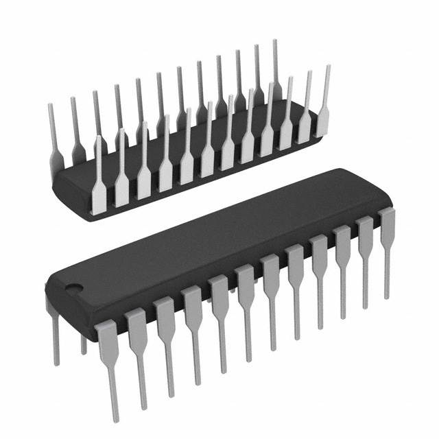
IC SCAN TEST DEVICE BUFF 24-DIP
Datasheet:
Delivery:


Payment:


In Stock : 0
Please send RFQ , we will respond immediately.


SN74BCT8244ANT Specifications
-
TypeParameter
-
Supplier Device Package24-PDIP
-
Package / Case24-DIP (0.300", 7.62mm)
-
Mounting TypeThrough Hole
-
Operating Temperature0°C ~ 70°C
-
Number of Bits8
-
Supply Voltage4.5V ~ 5.5V
-
Logic TypeScan Test Device with Buffers
-
PackagingTube
-
PackagingTube
-
Product StatusObsolete
-
Series74BCT
The 74AUP1T97GXZ is a single-gate configurable buffer/driver integrated circuit chip. It offers several advantages and can be used in various application scenarios. Some of the advantages and application scenarios of the 74AUP1T97GXZ are:Advantages: 1. Low power consumption: The chip operates at a low supply voltage (1.0V to 3.6V) and has a low power dissipation, making it suitable for battery-powered devices and energy-efficient applications. 2. High-speed operation: The chip has a high-speed propagation delay, enabling it to handle fast switching signals and high-frequency applications. 3. Configurable input/output voltage levels: The chip allows the user to configure the input and output voltage levels, making it compatible with different logic families and voltage levels. 4. Small form factor: The chip is available in a small package, making it suitable for space-constrained applications and compact electronic devices.Application Scenarios: 1. Level shifting: The configurable voltage levels of the chip make it suitable for level shifting applications, where signals need to be converted between different voltage domains or logic families. 2. Signal buffering: The chip can be used as a buffer or driver to amplify and shape digital signals, ensuring proper signal integrity and driving capability in various systems. 3. Interface conversion: The chip can be used to convert signals between different interfaces, such as TTL to CMOS or CMOS to LVDS, enabling compatibility between different electronic components. 4. Clock distribution: The chip's high-speed operation and low power consumption make it suitable for clock distribution applications, where precise and synchronized clock signals need to be distributed across a system. 5. Portable devices: Due to its low power consumption and small form factor, the chip can be used in portable devices like smartphones, tablets, wearables, and IoT devices, where power efficiency and compact size are crucial.These are just a few examples of the advantages and application scenarios of the 74AUP1T97GXZ integrated circuit chip. Its versatility and flexibility make it suitable for a wide range of digital logic applications.
SN74BCT8244ANT Relevant information
-
M38510/34201BEA
Texas Instruments -
SNJ54ABT18245AWD
Texas Instruments -
SNJ54LS181J
Texas Instruments -
M38510/34201BFA
Texas Instruments -
M38510/34201B2A
Texas Instruments -
SN54F283J
Texas Instruments -
SNJ54ABT18502HV
Texas Instruments -
SNJ54ABT8543FK
Texas Instruments -
M38510/07801BJA
Texas Instruments -
SNJ54BCT8245AJT
Texas Instruments