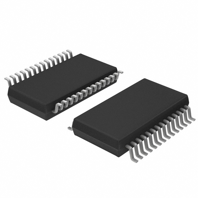
QS3390QG
Manufacturer No:
QS3390QG
Manufacturer:
Description:
IC MUX/DEMUX 1 X 16:8 28QSOP
Datasheet:
Delivery:


Payment:


In Stock : 0
Please send RFQ , we will respond immediately.


QS3390QG Specifications
-
TypeParameter
-
Supplier Device Package28-QSOP
-
Package / Case28-SSOP (0.154", 3.90mm Width)
-
Mounting TypeSurface Mount
-
Operating Temperature-40°C ~ 85°C
-
Voltage - Supply4.75V ~ 5.25V
-
Voltage Supply SourceSingle Supply
-
Current - Output High, Low-
-
Independent Circuits1
-
Circuit1 x 16:8
-
TypeMultiplexer/Demultiplexer
-
PackagingTube
-
Product StatusObsolete
-
Series-
The 74AC251SJX is a multiplexer/demultiplexer chip. It has 8 data input lines, a common select input, and two enable inputs. Here are the advantages and application scenarios of the 74AC251SJX integrated circuit chips:1. Advantages: a. High-speed operation: The 74AC251SJX operates at a high-speed AC performance, making it suitable for applications that require fast switching and processing of data. b. Wide operating voltage range: The chip can operate in a wide voltage range, typically from 2V to 6V, making it compatible with various power supply configurations. c. Low power consumption: The 74AC251SJX minimizes power consumption, making it suitable for battery-powered applications and energy-efficient designs. d. Compatibility: It is compatible with various logic families and can work seamlessly with other TTL-compatible devices. e. Compact and convenient: Being an integrated circuit chip, it offers a compact and space-saving solution for multiplexing and demultiplexing applications.2. Application scenarios: a. Data communication systems: The 74AC251SJX can be used in communication systems for data routing, multiplexing, or demultiplexing purposes. It can enable efficient data transmission and reception between different devices. b. Address decoding: It can be used as part of an address decoding system, allowing the selection of specific addresses or memory banks based on control signals. c. Data routing and selection: The chip can be used in digital systems to route data from multiple sources to a single destination or vice versa. It enables signal routing based on select inputs, allowing flexible data selection. d. Multiplexing and demultiplexing: The 74AC251SJX can be used to combine multiple data sources into a single stream (multiplexing) or to separate a multiplexed signal into individual data streams (demultiplexing). e. Bus systems: It can be used in bus systems to enable efficient data transfer between devices. The chip can act as a bus switch, allowing multiple devices to share a common bus line. f. Logic implementation: The 74AC251SJX can be used to implement various logical functions, such as logical AND/OR operations, based on the control signals and data inputs.Overall, the 74AC251SJX integrated circuit chips offer high-speed, low-power, and versatile solutions for various digital applications, including data communication, address decoding, multiplexing, and logic implementation.
QS3390QG Relevant information


