In Stock : 0
Please send RFQ , we will respond immediately.


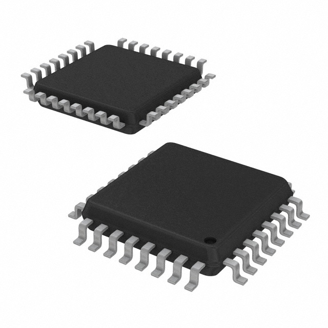
NB4L858MFAG Specifications
-
TypeParameter
-
Supplier Device Package32-LQFP (7x7)
-
Package / Case32-LQFP
-
Mounting TypeSurface Mount
-
Operating Temperature-40°C ~ 85°C
-
Voltage - Supply2.3V ~ 3.6V
-
Voltage Supply SourceSingle Supply
-
Current - Output High, Low-
-
Independent Circuits2
-
Circuit2 x 2:2
-
TypeCrosspoint Switch
-
PackagingTray
-
PackagingTray
-
Product StatusObsolete
-
Series-
The CD4527BK3 is a dual J-K flip-flop integrated circuit chip. It has several advantages and application scenarios, including:1. Dual Flip-Flop: The CD4527BK3 contains two independent J-K flip-flops in a single chip. This allows for compact circuit designs and reduces the number of components required.2. Versatile Functionality: The J-K flip-flop is a versatile sequential logic circuit that can be used for various applications such as frequency division, data synchronization, and control signal generation.3. Edge-Triggered Operation: The CD4527BK3 operates on the rising edge of the clock signal, which provides precise timing control and synchronization.4. Wide Operating Voltage Range: The chip can operate within a wide voltage range, typically from 3V to 18V. This makes it compatible with various power supply configurations.5. Low Power Consumption: The CD4527BK3 is designed to consume low power, making it suitable for battery-powered applications or energy-efficient designs.Application scenarios for the CD4527BK3 include:1. Frequency Division: The chip can be used to divide the frequency of an input signal by 2, 4, 8, or other factors, depending on the configuration of the J-K flip-flops. This is useful in applications such as clock signal generation or frequency scaling.2. Data Synchronization: The CD4527BK3 can be used to synchronize data signals with a clock signal. This is commonly used in digital communication systems to ensure accurate data transmission and reception.3. Control Signal Generation: The chip can generate control signals based on specific input conditions. This is useful in applications such as sequential logic circuits, counters, or state machines.4. Timing and Delay Circuits: The CD4527BK3 can be used to create precise timing and delay circuits. By controlling the clock signal and input conditions, it can introduce specific time delays or trigger events at precise intervals.5. Logic Circuit Design: The CD4527BK3 can be used as a building block in more complex logic circuit designs. By combining multiple flip-flops and other logic gates, it is possible to create custom logic functions or sequential circuits.Overall, the CD4527BK3 integrated circuit chip offers flexibility, compactness, and low power consumption, making it suitable for a wide range of digital logic applications.
NB4L858MFAG Relevant information


