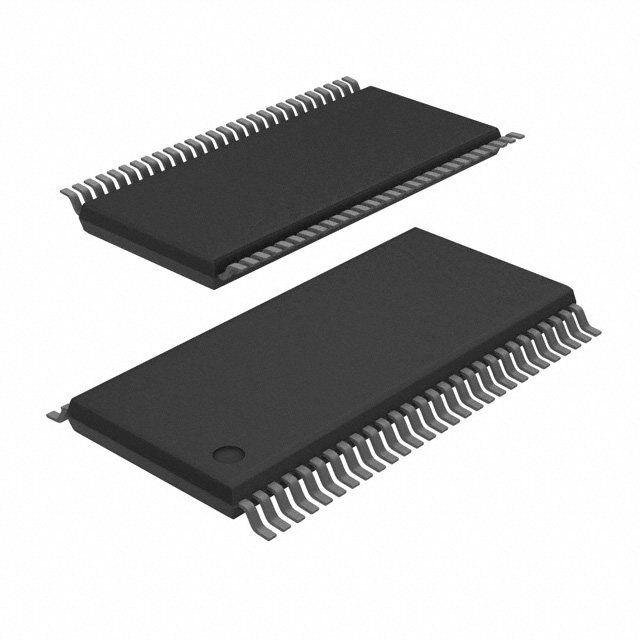
SN74CBTLV16292DLR
Manufacturer No:
SN74CBTLV16292DLR
Manufacturer:
Description:
IC MUX/DEMUX 12 X 1:2 56SSOP
Datasheet:
Delivery:


Payment:


In Stock : 0
Please send RFQ , we will respond immediately.


SN74CBTLV16292DLR Specifications
-
TypeParameter
-
Supplier Device Package56-SSOP
-
Package / Case56-BSSOP (0.295", 7.50mm Width)
-
Mounting TypeSurface Mount
-
Operating Temperature-40°C ~ 85°C
-
Voltage - Supply2.3V ~ 3.6V
-
Voltage Supply SourceSingle Supply
-
Current - Output High, Low-
-
Independent Circuits1
-
Circuit12 x 1:2
-
TypeMultiplexer/Demultiplexer
-
PackagingCut Tape (CT)
-
PackagingTape & Reel (TR)
-
Product StatusActive
-
Series74CBTLV
The SN74LVC139APWG4 is a dual 2-line to 4-line decoder/demultiplexer chip, and it offers several advantages and application scenarios. Here are some of them:Advantages: 1. Low-voltage operation: The chip operates at low-voltage levels (VCC = 1.65 V to 5.5 V), making it suitable for a wide range of low-power applications. 2. High-speed performance: It has a high-speed propagation delay of 3.8 ns (typical) at 3.3 V, making it suitable for applications requiring fast data processing. 3. Output drive capability: The output drive capability of the chip allows it to drive up to 10 LSTTL loads, or up to 15 pF of low-power Schottky loads. 4. Schmitt-trigger inputs: The inputs are equipped with Schmitt-trigger circuits, which provide hysteresis to improve noise immunity and provide better signal reception. 5. ESD protection: The chip is designed to have electrostatic discharge (ESD) protection, which increases its robustness and reliability.Application Scenarios: 1. Address decoding: The dual 2-line to 4-line decoder can be used for address decoding in microcontrollers, microprocessors, or other digital systems, where it selects a specific device or memory location based on the input address. 2. Data demultiplexing: It can be used to demultiplex an input data stream to multiple output lines based on the decoder logic, allowing for data distribution and routing in various applications. 3. Signal routing: The chip can be employed in applications where multiple input signals need to be routed selectively to different output lines or devices based on certain conditions or control signals. 4. Memory control: In memory systems, the SN74LVC139APWG4 can be utilized for controlling read/write operations, chip selection, or memory bank selection. 5. System control logic: The decoder/demultiplexer chip can serve as a component in various control logic circuits, such as sequencers, state machines, and digital control units.Please note that these are just a few examples, and the actual application scenarios may vary depending on the specific requirements and design considerations of a given system.
SN74CBTLV16292DLR Relevant information


