


Share
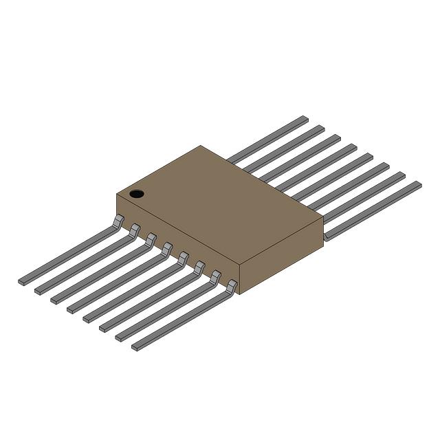

SNJ54AHC157W
Manufacturer No:
SNJ54AHC157W
Manufacturer:
Description:
54AHC157 QUADRUPLE 2-LINE TO 1-L
Datasheet:
Delivery:


Payment:


In Stock : 28
Please send RFQ , we will respond immediately.


SNJ54AHC157W Specifications
-
TypeParameter
-
Supplier Device Package-
-
Package / Case-
-
Mounting Type-
-
Operating Temperature-
-
Voltage - Supply-
-
Voltage Supply Source-
-
Current - Output High, Low-
-
Circuit-
-
Type-
-
PackagingBulk
-
Product StatusActive
-
Series*
The CD54HCT257F is a quad 2-input multiplexer (MUX) integrated circuit chip. Here are the advantages and application scenarios of this chip:Advantages:1. High-speed operation: The CD54HCT257F offers high-speed operation due to its HCT (High-Speed CMOS TTL compatible) technology. It can handle high-frequency signals and data switching efficiently.2. Low power consumption: This chip consumes very low power, making it suitable for battery-operated devices or low-power applications.3. Wide operating voltage range: It can operate within a wide voltage range, typically between 4.5V and 5.5V. This flexibility allows it to be used in various power supply environments.4. High noise immunity: The HCT technology provides high noise immunity, making the CD54HCT257F resistant to noise and interference during signal switching.Application scenarios:1. Data multiplexing: The CD54HCT257F is primarily used for data multiplexing. It has four independent MUX gates that can select one of the two data inputs (usually binary) and pass it to the output based on the select inputs. This functionality is useful in applications where multiple data sources need to be switched or selected for further processing.2. Address decoding: The multiplexing function of this chip can be used for address decoding purposes. It allows different memory or peripheral devices to be selected based on various combination inputs. This is commonly employed in microcontrollers or memory systems to enable efficient addressing of multiple devices.3. Signal routing: The CD54HCT257F can be used for routing analog or digital signals between different circuits or components, allowing flexibility in the signal path. It enables efficient switching and connection of different signal sources to the desired destination.4. Logic level conversion: As the chip is TTL compatible, it can be used for logic level conversion between CMOS and TTL logic families. This helps in interfacing different types of devices or systems with varying voltage requirements.5. Data selectors: The four independent MUX gates can act as data selectors, allowing the choice of input data based on the select inputs. This functionality finds applications in data processing systems where selective data transmission or manipulation is necessary.Overall, the CD54HCT257F integrated circuit chip is versatile and can be employed in various applications requiring data multiplexing, signal routing, address decoding, logic level conversion, or data selection.
SNJ54AHC157W Relevant information