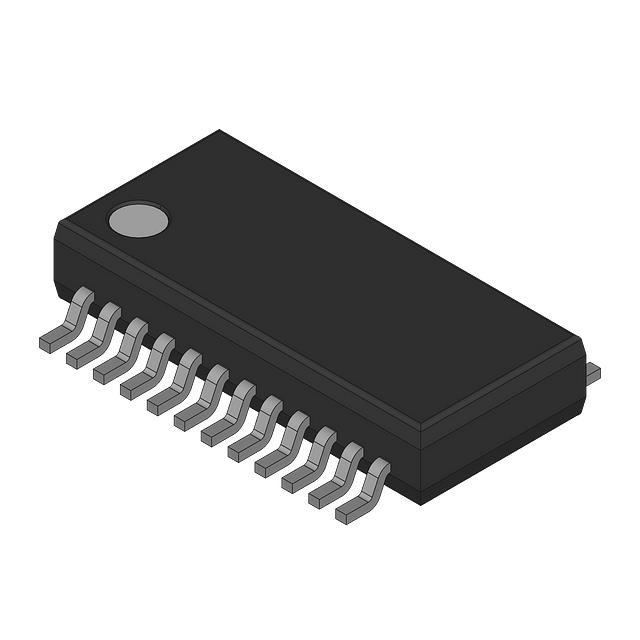
74CBTLV3384QG
Manufacturer No:
74CBTLV3384QG
Manufacturer:
Description:
IC BUS SWITCH 5 X 1:1 24QSOP
Datasheet:
Delivery:


Payment:


In Stock : 30145
Please send RFQ , we will respond immediately.


74CBTLV3384QG Specifications
-
TypeParameter
-
Supplier Device Package24-QSOP
-
Package / Case24-SSOP (0.154", 3.90mm Width)
-
Mounting TypeSurface Mount
-
Operating Temperature-40°C ~ 85°C
-
Voltage - Supply2.3V ~ 3.6V
-
Voltage Supply SourceSingle Supply
-
Current - Output High, Low-
-
Independent Circuits2
-
Circuit5 x 1:1
-
TypeBus Switch
-
PackagingBulk
-
Product StatusActive
-
Series74CBTLV
The SN74LS257BN3 is a quad 2-to-1 multiplexer integrated circuit chip. Here are the advantages and application scenarios of this chip:1. Space-saving: The SN74LS257BN3 integrates four 2-to-1 multiplexers in a single chip, leading to significant space savings on a circuit board.2. Cost-effective: Using a single SN74LS257BN3 chip to implement multiple 2-to-1 multiplexers reduces the overall cost compared to using individual components for each multiplexer.3. Versatility: This chip can be used for a wide range of applications that require multiplexing or data selection, such as data routing, signal selection, and interfacing different components.4. Fast operation: The chip operates at high speeds, making it suitable for applications that require quick data switching or selection.5. Low power consumption: SN74LS257BN3 is designed to operate with low power consumption, making it suitable for battery-powered or energy-efficient applications.6. Robustness: The chip is designed to withstand various environmental conditions and provides reliable performance over a wide range of temperatures.Application scenarios:1. Data routing: SN74LS257BN3 can be used to combine or route multiple data sources to a single output based on control signals. For example, it can be used in data bus multiplexing or selection in a microcontroller or digital system.2. Signal selection: In systems that require the selection of different signals based on certain criteria, the chip can be used to choose between multiple input signals and direct them to the desired output.3. Logical operations: The SN74LS257BN3 can also be used as a building block for logical operations. By using multiple chips in combination, complex logical functions can be implemented, such as binary arithmetic or data manipulation.4. Address decoding: The chip can be used for address decoding in memory systems or I/O interfaces, where multiple address lines need to be decoded to select a specific memory location or device.5. Communication systems: The chip can be used in communication systems to select different channels or inputs based on control signals.Overall, the SN74LS257BN3 proves advantageous in various scenarios where data selection, routing, or logical operations are required, and its integration and cost-effectiveness make it a popular choice for designers.
74CBTLV3384QG Relevant information


