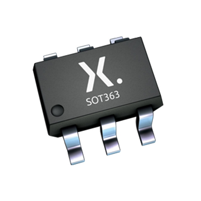
74LVC1G18GW-Q100H
Manufacturer No:
74LVC1G18GW-Q100H
Manufacturer:
Description:
IC DEMULTIPLEXER 1 X 1:2 6TSSOP
Datasheet:
Delivery:


Payment:


In Stock : 1482
Please send RFQ , we will respond immediately.


74LVC1G18GW-Q100H Specifications
-
TypeParameter
-
Independent Circuits1
-
Supplier Device Package6-TSSOP
-
Package / Case6-TSSOP, SC-88, SOT-363
-
Mounting TypeSurface Mount
-
Operating Temperature-40°C ~ 125°C
-
Voltage - Supply1.65V ~ 5.5V
-
Voltage Supply SourceSingle Supply
-
Current - Output High, Low32mA, 32mA
-
Circuit1 x 1:2
-
TypeDemultiplexer
-
PackagingCut Tape (CT)
-
PackagingTape & Reel (TR)
-
Product StatusActive
-
SeriesAutomotive, AEC-Q100, 74LVC
The 74LVC1G18GW-Q100H is a single gate buffer/driver integrated circuit chip. It offers several advantages and can be used in various application scenarios. Some of the advantages and application scenarios of this chip are:Advantages: 1. Low power consumption: The 74LVC1G18GW-Q100H operates at low power, making it suitable for battery-powered devices and energy-efficient applications. 2. Wide operating voltage range: It can operate within a wide voltage range, typically from 1.65V to 5.5V, allowing compatibility with different voltage levels. 3. High-speed operation: This chip has a high-speed operation capability, making it suitable for applications that require fast switching and signal transmission. 4. Schmitt-trigger input: The Schmitt-trigger input feature ensures a hysteresis effect, providing noise immunity and stable operation in noisy environments. 5. Small form factor: The chip is available in a small package, making it suitable for space-constrained applications and compact designs.Application Scenarios: 1. Signal buffering: The 74LVC1G18GW-Q100H can be used to buffer and amplify digital signals, ensuring signal integrity and driving capability in various digital systems. 2. Level shifting: It can be used for level shifting applications, where signals need to be converted from one voltage level to another, ensuring compatibility between different voltage domains. 3. Clock distribution: The chip can be used for clock distribution in digital systems, ensuring accurate and synchronized clock signals across multiple components. 4. Sensor interfaces: It can be used in sensor interfaces to buffer and condition sensor signals, ensuring reliable and accurate data acquisition. 5. Communication systems: The chip can be used in communication systems, such as UART, SPI, or I2C interfaces, to buffer and drive signals between different components.These are just a few examples of the advantages and application scenarios of the 74LVC1G18GW-Q100H integrated circuit chip. Its versatility, low power consumption, and small form factor make it suitable for a wide range of digital applications.
74LVC1G18GW-Q100H Relevant information


