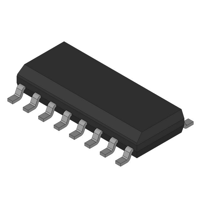
SN74LVC257ADB
Manufacturer No:
SN74LVC257ADB
Manufacturer:
Description:
MUX, 2 LINE INPUT
Datasheet:
Delivery:


Payment:


In Stock : 9120
Please send RFQ , we will respond immediately.


SN74LVC257ADB Specifications
-
TypeParameter
-
Supplier Device Package16-SSOP
-
Package / Case16-SSOP (0.209", 5.30mm Width)
-
Mounting TypeSurface Mount
-
Operating Temperature-40°C ~ 85°C
-
Voltage - Supply1.65V ~ 3.6V
-
Voltage Supply SourceSingle Supply
-
Current - Output High, Low24mA, 24mA
-
Independent Circuits1
-
Circuit4 x 2:1
-
TypeMultiplexer
-
PackagingBulk
-
Product StatusActive
-
Series74LVC
The SN74LVC257ADB is a quad 2-input multiplexer/demultiplexer integrated circuit chip. It offers several advantages and can be used in various application scenarios. Some of the advantages and application scenarios of the SN74LVC257ADB are:Advantages: 1. Low voltage operation: The chip operates at a low voltage range of 1.65V to 5.5V, making it suitable for low-power applications. 2. High-speed operation: It has a high-speed propagation delay of 3.8 ns, enabling fast data switching. 3. Low power consumption: The chip has low power consumption, making it energy-efficient. 4. Wide operating temperature range: It can operate in a wide temperature range of -40°C to 125°C, making it suitable for various environments. 5. ESD protection: The chip provides ESD protection, ensuring reliability and durability.Application Scenarios: 1. Data multiplexing: The SN74LVC257ADB can be used to select one of four data inputs and route it to a single output. This is useful in applications where multiple data sources need to be switched or combined. 2. Data demultiplexing: It can also be used to take a single input and route it to one of four outputs. This is useful in applications where a single data source needs to be distributed to multiple destinations. 3. Address decoding: The chip can be used for address decoding in microcontrollers or memory systems. It can select one of multiple memory or peripheral devices based on the address input. 4. Data routing and switching: The SN74LVC257ADB can be used to route or switch data between different components or subsystems in a digital system. 5. Logic level conversion: It can be used to convert logic levels between different voltage domains, allowing compatibility between devices operating at different voltage levels.Overall, the SN74LVC257ADB offers versatility, low power consumption, and high-speed operation, making it suitable for a wide range of applications in digital systems.
SN74LVC257ADB Relevant information


