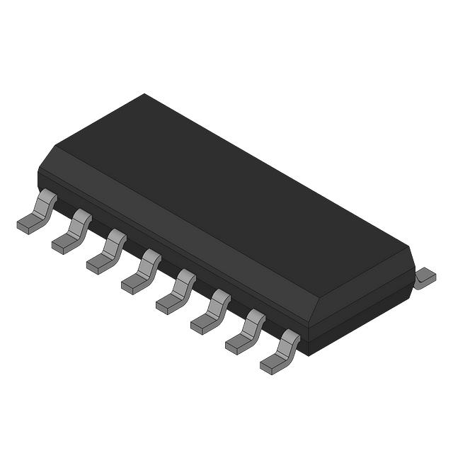
CD74FCT157ATNM96
Manufacturer No:
CD74FCT157ATNM96
Manufacturer:
Description:
FAST CMOS QUAD 2-INPUT MUXS
Datasheet:
Delivery:


Payment:


In Stock : 3000
Please send RFQ , we will respond immediately.


CD74FCT157ATNM96 Specifications
-
TypeParameter
-
Supplier Device Package16-SOIC
-
Package / Case16-SOIC (0.154", 3.90mm Width)
-
Mounting TypeSurface Mount
-
Operating Temperature-40°C ~ 85°C
-
Voltage - Supply4.75V ~ 5.25V
-
Voltage Supply SourceSingle Supply
-
Current - Output High, Low15mA, 48mA
-
Independent Circuits1
-
Circuit4 x 2:1
-
TypeMultiplexer
-
PackagingBulk
-
Product StatusObsolete
-
Series-
The CD74FCT157ATNM96 is a quad 2-input multiplexer with complementary outputs, and it is a part of the FCT family of integrated circuit chips. Here are some advantages and application scenarios of the CD74FCT157ATNM96:Advantages: 1. Fast Operation: The FCT family of chips are known for their high-speed performance, with propagation delays as low as 4.5 ns. This makes them suitable for applications that require quick switching and response times. 2. Compatibility: The CD74FCT157ATNM96 is designed to be directly interchangeable with similar industry-standard 74F and 74ALS parts. This means it can easily replace or be replaced by other chips in a circuit without any significant modifications. 3. Low Power Consumption: FCT chips are built using low-power CMOS technology, which helps in reducing the power consumption while maintaining high performance. 4. Wide Operating Voltage Range: The CD74FCT157ATNM96 can function with a wide operating voltage range, typically between 4.5V to 5.5V. This flexibility allows it to be used in various applications that require different voltage levels.Application Scenarios: 1. Data Multiplexing: The CD74FCT157ATNM96 can select one of four data input sources and drive the selected data onto its output line. This makes it useful in applications where data from multiple sources needs to be combined or switched. 2. Address Selection: In memory systems or address decoding circuits, the CD74FCT157ATNM96 can be used to select one of multiple address input signals to drive the output for address decoding and data routing purposes. 3. Bus Switching: It can be employed in bus interfaces to switch between different data buses or to control the direction of data flow. 4. Control Signal Routing: The chip can be used to select and route control signals in various digital systems, enabling efficient control of system operation.Overall, the CD74FCT157ATNM96 chip's fast operation, compatibility, low power consumption, and wide operating voltage range make it suitable for a range of applications requiring data multiplexing, address selection, bus switching, and control signal routing.
CD74FCT157ATNM96 Relevant information


