


Share

In Stock : 0
Please send RFQ , we will respond immediately.


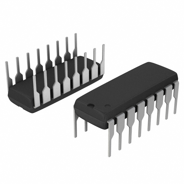
CD4015BCN Specifications
-
TypeParameter
-
Supplier Device Package16-PDIP
-
Package / Case16-DIP (0.300", 7.62mm)
-
Mounting TypeThrough Hole
-
Operating Temperature-55°C ~ 125°C
-
Voltage - Supply3V ~ 18V
-
FunctionSerial to Parallel
-
Number of Bits per Element4
-
Number of Elements2
-
Output TypeComplementary
-
Logic TypeShift Register
-
PackagingTube
-
Product StatusObsolete
-
Series4000B
The CD4015BCN is a dual 4-bit static shift register integrated circuit chip. Some of the advantages and application scenarios of this chip include:1. Simple design: The CD4015BCN is a fairly straightforward IC chip with a relatively simple design, making it easy to use and integrate into circuits.2. Serial-to-parallel conversion: The chip can convert serial data input into parallel output, making it useful for applications where data needs to be processed in parallel.3. Shift register functionality: The CD4015BCN can shift data in either direction (right or left), allowing for various operations such as data storage, data transfer, or pattern generation.4. Control inputs: The chip has control inputs that allow selective parallel loading and individual clocking of the flip-flops, providing flexibility and control over data manipulation.5. Cascading: Multiple CD4015BCN chips can be cascaded together to increase the number of shift registers in a system, accommodating larger data sets or more complex applications.Application scenarios:1. Data storage and transfer: The CD4015BCN can be used to store data in its flip-flops and subsequently transfer it serially or in parallel to other components in a circuit.2. Serial data reception: The chip can receive and convert serial data into parallel form, which is useful in applications such as UART (Universal Asynchronous Receiver-Transmitter) communication.3. Shift register operations: The CD4015BCN can be used to perform various shift register operations like shifting data, serial-to-parallel conversion, parallel-to-serial conversion, arithmetic operations, and more.4. Pattern generation: By continuously shifting data in the chip, it can be utilized to generate specific patterns or sequences of data.5. Logic circuit design: The CD4015BCN can be incorporated into larger logic circuits for tasks like data synchronization, data sequencing, or data distribution.It's important to note that while the CD4015BCN has its advantages and application scenarios, the specific implementation and usage will depend on the overall circuit design and requirements.
CD4015BCN Relevant information