


Share

74F675ASC
Manufacturer No:
74F675ASC
Manufacturer:
Description:
SERIAL IN PARALLEL OUT
Datasheet:
Delivery:


Payment:


In Stock : 955
Please send RFQ , we will respond immediately.


74F675ASC Specifications
-
TypeParameter
-
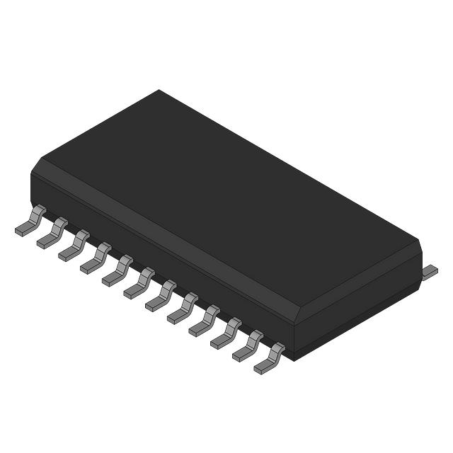
Supplier Device Package24-SOP
-
Package / Case24-SOIC (0.295", 7.50mm Width)
-
Mounting TypeSurface Mount
-
Operating Temperature0°C ~ 70°C
-
Voltage - Supply4.5V ~ 5.5V
-
FunctionSerial to Parallel, Serial
-
Number of Bits per Element16
-
Number of Elements1
-
Output TypeTri-State
-
Logic TypeShift Register
-
PackagingTube
-
Product StatusObsolete
-
Series74F
The 74F675ASC is a 16-bit edge-triggered register with three-state outputs, which is a type of integrated circuit chip. Some advantages and application scenarios of this chip are:Advantages: 1. High-speed operation: The 74F675ASC chip is designed for high-speed applications, making it suitable for use in systems that require fast data transfer and processing. 2. Edge-triggered design: The chip is edge-triggered, meaning it captures and stores data only when a specific edge (rising or falling) of the clock signal occurs. This allows for precise control and synchronization of data transfer. 3. Three-state outputs: The chip has three-state outputs, which means it can be in one of three states: high, low, or high impedance. This feature enables multiple chips to be connected together without causing conflicts or bus contention.Application scenarios: 1. Data storage and transfer: The 74F675ASC chip can be used as a register to store and transfer data in various digital systems, such as microprocessors, microcontrollers, and digital signal processors. 2. Parallel data processing: With its 16-bit capacity, the chip is suitable for parallel data processing applications, where multiple bits of data need to be processed simultaneously. 3. Bus interfacing: The three-state outputs of the chip make it useful for interfacing with buses or data lines in a system. It can be used to drive or receive data from a shared bus, allowing multiple devices to communicate with each other. 4. Control and synchronization: The edge-triggered design of the chip makes it suitable for control and synchronization applications, where precise timing and sequencing of events are required.Overall, the 74F675ASC integrated circuit chip offers high-speed operation, edge-triggered design, and three-state outputs, making it useful in various applications involving data storage, transfer, parallel processing, bus interfacing, and control/synchronization.
74F675ASC Relevant information