


Share

CD4094BNSR
Manufacturer No:
CD4094BNSR
Manufacturer:
Description:
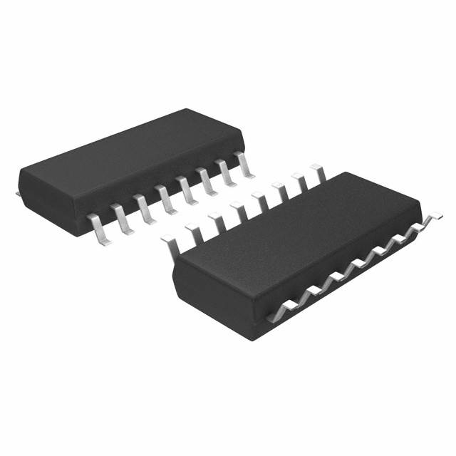
IC SHIFT/STORE BUS REGSTR 16SO
Datasheet:
Delivery:


Payment:


In Stock : 990
Please send RFQ , we will respond immediately.


CD4094BNSR Specifications
-
TypeParameter
-
Supplier Device Package16-SO
-
Package / Case16-SOIC (0.209", 5.30mm Width)
-
Mounting TypeSurface Mount
-
Operating Temperature-55°C ~ 125°C
-
Voltage - Supply3V ~ 18V
-
FunctionSerial to Parallel
-
Number of Bits per Element8
-
Number of Elements1
-
Output TypeTri-State
-
Logic TypeShift Register
-
PackagingCut Tape (CT)
-
PackagingTape & Reel (TR)
-
Product StatusActive
-
Series4000B
The CD4094BNSR is a popular integrated circuit (IC) chip that serves as an 8-bit shift register/latch. Here are some advantages and application scenarios of the CD4094BNSR:1. Simple implementation: The CD4094BNSR provides a straightforward and easy-to-use solution for shifting and latching data bits. It requires minimal external components and can be easily integrated into digital systems.2. Serial-to-parallel data conversion: The chip allows conversion of serial input data into parallel output data. It can receive serial data and then shift it into its internal memory, which can then be latched and stored in parallel form for further processing.3. Control over data timing: The CD4094BNSR features a Clock (CLK) pin that enables precise control over the shifting and latching of data. This allows synchronization and proper timing of data flow within a system, ensuring reliable and accurate data handling.4. Cascading capability: Multiple CD4094BNSR chips can be easily cascaded together to increase the number of output bits. This makes it suitable for applications where more than 8 bits of parallel output are required, such as LED displays, LED matrices, or motor control systems.5. Low power consumption: The CD4094BNSR has low power consumption, making it suitable for battery-powered devices or energy-efficient applications.6. Versatile applications: The CD4094BNSR finds applications in various electronic systems and projects, including LED displays, seven-segment displays, LED matrices, digital clocks, data multiplexing, robotics, and general-purpose data shifting/general-purpose input and output (GPIO) expansion.Overall, the CD4094BNSR provides a convenient solution for serial-to-parallel data conversion, allowing accurate control over data shifting and latching. Its simplicity, cascading capability, and low power consumption make it suitable for various digital applications.
CD4094BNSR Relevant information