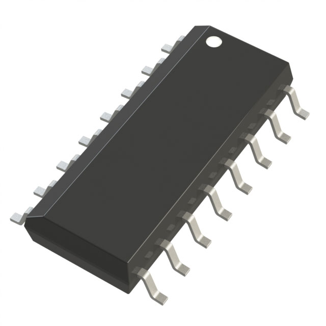
74HC259D-Q100,118
Manufacturer No:
74HC259D-Q100,118
Manufacturer:
Description:
IC LATCH 8BIT ADDRESS 16SOIC
Datasheet:
Delivery:


Payment:


In Stock : 0
Please send RFQ , we will respond immediately.


74HC259D-Q100,118 Specifications
-
TypeParameter
-
Supplier Device Package16-SO
-
Package / Case16-SOIC (0.154", 3.90mm Width)
-
Mounting TypeSurface Mount
-
Operating Temperature-40°C ~ 125°C
-
Current - Output High, Low5.2mA, 5.2mA
-
Delay Time - Propagation17ns
-
Independent Circuits1
-
Voltage - Supply2V ~ 6V
-
Output TypeStandard
-
Circuit1:8
-
Logic TypeD-Type, Addressable
-
PackagingCut Tape (CT)
-
PackagingTape & Reel (TR)
-
Product StatusActive
-
SeriesAutomotive, AEC-Q100, 74HC
The 74HC259D-Q100,118 integrated circuit chip is a 8-bit addressable latch with output enable. Here are some advantages and application scenarios of this chip:Advantages: 1. High-speed operation: The chip operates at high speeds, making it suitable for applications that require fast data storage and retrieval.2. Wide operating voltage range: The chip can operate within a wide voltage range, typically from 2V to 6V, providing flexibility in various circuit designs.3. Output enable feature: The chip has an output enable pin that allows the user to control the output status of the latch. This feature enables multiplexing and data storage.4. Addressable latch: The chip features 8-bit addressable latch functionality, allowing the user to store and access data at specific addresses, which is useful in applications such as memory expansion, data buffering, and address decoding.Application scenarios: 1. Memory expansion: The 74HC259D-Q100,118 can be used to expand the memory of microcontrollers or other digital systems by storing data at different addressable locations.2. Address decoding: The chip can be used to decode addresses in memory mapping applications. By storing relevant information at specific addresses, the chip enables efficient address decoding for interfacing with different peripherals.3. Multiplexing: The output enable feature of the chip can be utilized to multiplex multiple data sources. By enabling/disabling the latch outputs as needed, the chip allows the routing of different data streams to a single output line.4. Data buffering: The chip can be used as a buffer to store data temporarily and control its timing. It can be particularly useful in applications where data transfer rates between different devices vary.5. Control circuitry: The latch functionality of the chip can be used to store control signals, enabling efficient control and synchronization of different operations in complex digital systems.Overall, the 74HC259D-Q100,118 integrated circuit chip offers advantages such as high-speed operation, wide voltage range, and addressable latch functionality, making it suitable for various applications requiring data storage, multiplexing, addressing, and control.
74HC259D-Q100,118 Relevant information
-
SNJ54ALS580BW
Texas Instruments -
M38510/34601BRA
Texas Instruments -
SNJ54HC573AW
Texas Instruments -
SN54ALS259J
Texas Instruments -
M38510/65406BRA
Texas Instruments -
M38510/65453BSA
Texas Instruments -
M38510/38201B2A
Texas Instruments -
M38510/65403BRA
Texas Instruments -
SNJ54ALS996JT
Texas Instruments -
SNJ54AHCT373J
Texas Instruments


