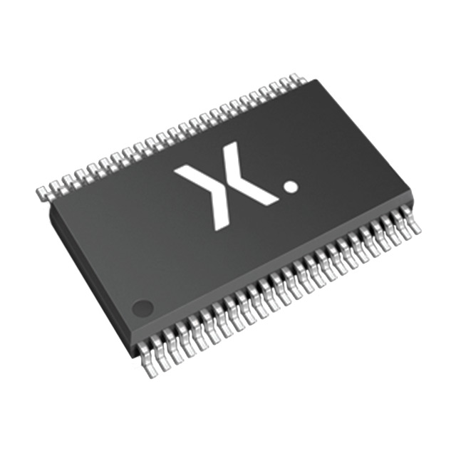
74LVCH16373ADGG:11
Manufacturer No:
74LVCH16373ADGG:11
Manufacturer:
Description:
IC TRANSP LATCH TRI-ST 48TSSOP
Datasheet:
Delivery:


Payment:


In Stock : 661
Please send RFQ , we will respond immediately.


74LVCH16373ADGG:11 Specifications
-
TypeParameter
-
Supplier Device Package48-TSSOP
-
Package / Case48-TFSOP (0.240", 6.10mm Width)
-
Mounting TypeSurface Mount
-
Operating Temperature-40°C ~ 125°C
-
Current - Output High, Low24mA, 24mA
-
Delay Time - Propagation1.5ns
-
Independent Circuits2
-
Voltage - Supply1.2V ~ 3.6V
-
Output TypeTri-State
-
Circuit8:8
-
Logic TypeD-Type Transparent Latch
-
PackagingCut Tape (CT)
-
PackagingTape & Reel (TR)
-
Product StatusActive
-
Series74LVCH
The 74LVCH16373ADGG:11 is a 16-bit transparent D-type latch integrated circuit chip with 3-state outputs. Here are some advantages and application scenarios of this chip:Advantages: 1. High-speed operation: The 74LVCH16373ADGG:11 chip operates at very high speeds, making it suitable for applications requiring quick and efficient data transfer. 2. Low power consumption: This chip is designed to consume minimal power, making it energy-efficient and suitable for portable devices or battery-powered applications. 3. Wide operating voltage range: The chip operates within a wide voltage range (1.65V to 5.5V), allowing compatibility with various digital systems and voltage levels. 4. 3-state outputs: The 74LVCH16373ADGG:11 chip has 3-state outputs, which means it can be placed in a high-impedance state when not actively driving signals. This feature enables easy interfacing with a multi-drop bus or multiple devices.Application scenarios: 1. Data storage and transfer: The 74LVCH16373ADGG:11 chip can be used as a data buffer for storing and transferring 16-bit digital data. It is commonly used in applications such as data communication systems, memory modules, and data routing. 2. Registers and latches: The chip can be used to build registers and latches in digital systems for temporary data storage or synchronization purposes. It is suitable for applications like digital clock circuits, counters, and synchronization of multiple signals. 3. Bus interfacing: With its 3-state outputs, the chip can be utilized as a bus transceiver or interface in systems where multiple devices need to share data on a common bus. It helps in controlling the bus access and managing data flow. 4. FPGA and microcontroller interface: The chip can be employed as an interface between Field-Programmable Gate Arrays (FPGAs), microcontrollers, or other digital devices, enabling communication and data exchange between them.Note: It's essential to carefully review the datasheet and verify the specific capabilities, pin configuration, voltage requirements, and operating conditions of the 74LVCH16373ADGG:11 chip before integrating it into a design.
74LVCH16373ADGG:11 Relevant information
-
SNJ54ALS580BW
Texas Instruments -
M38510/34601BRA
Texas Instruments -
SNJ54HC573AW
Texas Instruments -
SN54ALS259J
Texas Instruments -
M38510/65406BRA
Texas Instruments -
M38510/65453BSA
Texas Instruments -
M38510/38201B2A
Texas Instruments -
M38510/65403BRA
Texas Instruments -
SNJ54ALS996JT
Texas Instruments -
SNJ54AHCT373J
Texas Instruments


