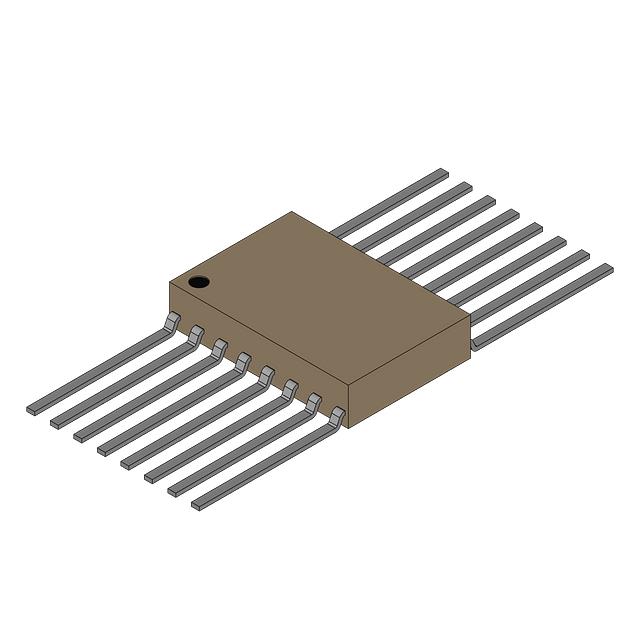
CD4099BK
Manufacturer No:
CD4099BK
Manufacturer:
Description:
CMOS 8-BIT ADDRESSABLE LATCH
Datasheet:
Delivery:


Payment:


In Stock : 73
Please send RFQ , we will respond immediately.


CD4099BK Specifications
-
TypeParameter
-
Supplier Device Package16-CFP
-
Package / Case16-CFlatPack
-
Mounting TypeSurface Mount
-
Operating Temperature-55°C ~ 125°C
-
Current - Output High, Low6.8mA
-
Delay Time - Propagation50ns
-
Independent Circuits1
-
Voltage - Supply3V ~ 18V
-
Output TypeStandard
-
Circuit1:8
-
Logic TypeD-Type, Addressable
-
PackagingBulk
-
Product StatusActive
-
Series-
The CD4099BK is a versatile integrated circuit chip that offers various advantages and can be applied in different scenarios. Some of its advantages and application scenarios are:1. Versatility: The CD4099BK is a 8-bit universal shift/register capable of shifting in both directions. It can be configured as a serial-in, parallel-out (SIPO) shift register, a parallel-in, serial-out (PISO) shift register, or a bidirectional shift register. This versatility makes it suitable for a wide range of applications.2. Serial and parallel data transfer: The CD4099BK allows for efficient serial-to-parallel or parallel-to-serial data transfer. This feature is useful in applications that require conversion between different data formats or synchronization of multiple data streams.3. Cascade capability: Multiple CD4099BK chips can be cascaded together to increase the number of bits. This cascading capability makes it suitable for applications that involve large amounts of data processing or storage.4. Control logic flexibility: The CD4099BK includes control inputs such as Clock (CLK), Clear (CLR), and Shift/Load (SH/LD). These control inputs provide flexibility in controlling the data transfer and enable various operation modes. It can be easily integrated into different digital systems.5. Storage capability: The CD4099BK can be used as a temporary storage device. It allows parallel loading of data into the shift register, which can then be shifted out or maintained in the register until needed. This makes it useful in applications that require data buffering or temporary storage.6. Shift register applications: The CD4099BK can be applied in various scenarios that require serial data manipulation, such as data communication systems, serial-to-parallel converters, parallel-to-serial converters, digital displays, and data logging devices.7. Arithmetic operations: The versatile features of the CD4099BK can also be utilized in performing arithmetic operations. By combining multiple chips and implementing specific control logic, serial or parallel addition, subtraction, or other arithmetic operations can be achieved.In summary, the CD4099BK integrated circuit chip offers versatility in data transfer, storage, and control. Its ability to perform serial and parallel data manipulation, cascade capability, and storage functionality make it suitable for a wide range of applications involving data processing, conversion, and storage.
CD4099BK Relevant information
-
SNJ54ALS580BW
Texas Instruments -
M38510/34601BRA
Texas Instruments -
SNJ54HC573AW
Texas Instruments -
SN54ALS259J
Texas Instruments -
M38510/65406BRA
Texas Instruments -
M38510/65453BSA
Texas Instruments -
M38510/38201B2A
Texas Instruments -
M38510/65403BRA
Texas Instruments -
SNJ54ALS996JT
Texas Instruments -
SNJ54AHCT373J
Texas Instruments


