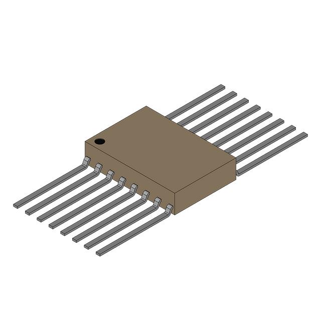
54LS259FMQB
Manufacturer No:
54LS259FMQB
Manufacturer:
Description:
D LATCH, LS SERIES TTL
Datasheet:
Delivery:


Payment:


In Stock : 772
Please send RFQ , we will respond immediately.


54LS259FMQB Specifications
-
TypeParameter
-
Supplier Device Package16-CFlatPack
-
Package / Case16-CFlatpack
-
Mounting TypeSurface Mount
-
Operating Temperature-55°C ~ 125°C
-
Current - Output High, Low400µA, 4mA
-
Delay Time - Propagation30ns
-
Independent Circuits1
-
Voltage - Supply4.5V ~ 5.5V
-
Output TypeComplementary
-
Circuit1:8
-
Logic TypeD-Type, Addressable
-
PackagingBulk
-
Product StatusActive
-
Series54LS
The 54LS259FMQB is a high-speed, low-power, and non-inverting integrated circuit chip that contains a storage register and a 3-state output buffer. Here are some advantages and application scenarios of this chip:Advantages:1. High-speed operation: The chip operates at a high speed, making it suitable for applications that require quick data transfer and processing.2. Low power consumption: The 54LS259FMQB chip has a low power design, making it energy-efficient and suitable for battery-powered devices or applications where power consumption is a concern.3. 3-state output buffer: The chip includes a 3-state output buffer that allows seamless interfacing with other devices or circuits. This functionality enables multiple chips to be connected together without causing bus contention.4. Multiple control inputs: The chip features multiple control inputs, such as enable and clear inputs, which enhance its flexibility and allow for versatile usage in various applications.Application scenarios:1. Address decoding: The chip can be used for address decoding in microprocessor-based systems. It can store and latch the address inputs, and its output can be used to activate specific memory or I/O devices based on the decoded address.2. Data storage and transfer: The chip can be used as a storage register to store and transfer data between different sections or stages of a circuit. It can hold the data until it is required and then transfer it to the desired destination.3. Multiplexing: The chip can be used in multiplexing applications where multiple signals need to be combined or switched to a single output. The storage register can hold different data inputs, and the chip's control inputs can be used to select and transfer the desired data to the output.4. Bus interface: The chip can be used as a buffer in data bus systems. Its 3-state output buffer allows it to drive the data bus without interfering with other devices connected to the same bus.5. Control circuitry: The chip can be used for implementing control circuitry in various electronic systems. Its multiple control inputs can be utilized to control different aspects of the system operation based on specific conditions or inputs.These are just a few examples of the advantages and application scenarios of the 54LS259FMQB integrated circuit chips. The actual usage can vary depending on the specific requirements of the system or project.
54LS259FMQB Relevant information
-
SNJ54ALS580BW
Texas Instruments -
M38510/34601BRA
Texas Instruments -
SNJ54HC573AW
Texas Instruments -
SN54ALS259J
Texas Instruments -
M38510/65406BRA
Texas Instruments -
M38510/65453BSA
Texas Instruments -
M38510/38201B2A
Texas Instruments -
M38510/65403BRA
Texas Instruments -
SNJ54ALS996JT
Texas Instruments -
SNJ54AHCT373J
Texas Instruments


