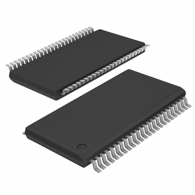
SN74LVC16373ADGVR
Manufacturer No:
SN74LVC16373ADGVR
Manufacturer:
Description:
IC TRANS D-TYP LATCH 3ST 48TVSOP
Datasheet:
Delivery:


Payment:


In Stock : 4616
Please send RFQ , we will respond immediately.


SN74LVC16373ADGVR Specifications
-
TypeParameter
-
Supplier Device Package48-TVSOP
-
Package / Case48-TFSOP (0.173", 4.40mm Width)
-
Mounting TypeSurface Mount
-
Operating Temperature-40°C ~ 85°C
-
Current - Output High, Low24mA, 24mA
-
Delay Time - Propagation2.1ns
-
Independent Circuits2
-
Voltage - Supply1.65V ~ 3.6V
-
Output TypeTri-State
-
Circuit8:8
-
Logic TypeD-Type Transparent Latch
-
PackagingCut Tape (CT)
-
PackagingTape & Reel (TR)
-
Product StatusActive
-
Series74LVC
The SN74LVC16373ADGVR is a 16-bit transparent D-type latch with 3-state outputs. It has several advantages and application scenarios, including:1. High-speed operation: The SN74LVC16373ADGVR operates at a high speed, making it suitable for applications that require fast data transfer and processing.2. Low power consumption: This integrated circuit chip is designed to consume low power, making it ideal for battery-powered devices or applications where power efficiency is crucial.3. 3-state outputs: The 3-state outputs allow multiple devices to share a common bus, enabling efficient data transfer and communication between different components.4. Wide operating voltage range: The SN74LVC16373ADGVR can operate within a wide voltage range, making it compatible with various power supply systems.5. ESD protection: The chip provides Electrostatic Discharge (ESD) protection, safeguarding it against potential damage from static electricity.Application scenarios for the SN74LVC16373ADGVR include:1. Data storage and transfer: The latch can be used to store and transfer data in various digital systems, such as microcontrollers, memory modules, and communication devices.2. Bus interfacing: The 3-state outputs make it suitable for bus interfacing applications, where multiple devices need to share a common data bus.3. Address decoding: The latch can be used in address decoding circuits to select specific memory locations or peripheral devices in a system.4. Control signal buffering: The chip can be used to buffer control signals in complex digital systems, ensuring proper signal integrity and preventing signal degradation.5. FPGA and ASIC designs: The SN74LVC16373ADGVR can be integrated into Field-Programmable Gate Arrays (FPGAs) or Application-Specific Integrated Circuits (ASICs) to provide data storage and transfer capabilities.Overall, the SN74LVC16373ADGVR offers high-speed operation, low power consumption, and versatile applications, making it a suitable choice for various digital systems and electronic devices.
SN74LVC16373ADGVR Relevant information
-
SNJ54ALS580BW
Texas Instruments -
M38510/34601BRA
Texas Instruments -
SNJ54HC573AW
Texas Instruments -
SN54ALS259J
Texas Instruments -
M38510/65406BRA
Texas Instruments -
M38510/65453BSA
Texas Instruments -
M38510/38201B2A
Texas Instruments -
M38510/65403BRA
Texas Instruments -
SNJ54ALS996JT
Texas Instruments -
SNJ54AHCT373J
Texas Instruments


