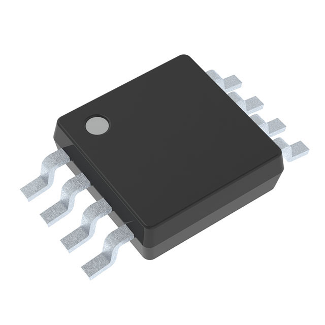
SN74LVC1G99QDCURQ1
Manufacturer No:
SN74LVC1G99QDCURQ1
Manufacturer:
Description:
IC CONFIG MULT-FUNC GATE US8
Datasheet:
Delivery:


Payment:


In Stock : 2318
Please send RFQ , we will respond immediately.


SN74LVC1G99QDCURQ1 Specifications
-
TypeParameter
-
Supplier Device Package8-VSSOP
-
Package / Case8-VFSOP (0.091", 2.30mm Width)
-
Mounting TypeSurface Mount
-
Operating Temperature-40°C ~ 125°C
-
Voltage - Supply1.65V ~ 5.5V
-
Current - Output High, Low32mA, 32mA
-
Output TypeTri-State
-
Schmitt Trigger InputNo
-
Number of Inputs4
-
Number of Circuits1
-
Logic TypeConfigurable Multiple Function
-
PackagingCut Tape (CT)
-
PackagingTape & Reel (TR)
-
Product StatusActive
-
SeriesAutomotive, AEC-Q100, 74LVC
The SN74LVC1G99QDCURQ1 is a single buffer/line driver with 3-state output integrated circuit chip. It is designed for voltage level shifting and signal buffering in various applications. Here are some advantages and application scenarios of the SN74LVC1G99QDCURQ1:Advantages:1. Small package size: The chip is available in a very small and space-saving SOT-553 package, making it suitable for applications with limited board space.2. Wide operating voltage range: The chip operates from 1.65V to 5.5V, allowing compatibility with multiple voltage systems.3. 3-state output: The chip provides a 3-state output, allowing the buffer to be disconnected from the bus when not needed. This feature helps reduce power consumption and avoids bus contention issues.4. High-speed operation: The SN74LVC1G99QDCURQ1 chip is capable of high-speed switching, making it suitable for data and control signal buffering in applications that require fast response times.Application scenarios:1. Interface level shifting: The chip can be used for level shifting between different voltage domains in mixed-signal and mixed-voltage systems. It ensures proper signal communication between devices operating at different voltage levels.2. Signal buffering: The SN74LVC1G99QDCURQ1 chip can be employed for buffering and amplifying digital signals, maintaining signal integrity and driving capacitive loads. It is useful in applications where signals need to be conveyed over long distances or transmitted to multiple devices.3. Bus isolation: In scenarios where multiple devices share a common communication bus, the chip's 3-state output can be utilized for bus isolation. It allows multiple devices to connect to the bus without interfering with the transmissions of other devices.4. Level translation: When interfacing between different logic families or voltage levels, the chip can be used to translate signals from one voltage level to another. This makes it compatible with systems that use different logic voltages.Overall, the SN74LVC1G99QDCURQ1 integrated circuit chip offers small size, wide voltage range, high-speed operation, and 3-state output capabilities. These features make it suitable for various applications that require level shifting, signal buffering, and signal isolation in both mixed-voltage and mixed-signal systems.
SN74LVC1G99QDCURQ1 Relevant information


