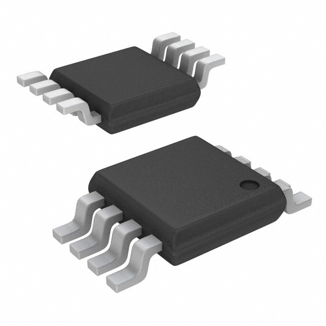
XC7WT14DP,125
Manufacturer No:
XC7WT14DP,125
Manufacturer:
Description:
IC INVERT SCHMITT 3CH 3IN 8TSSOP
Datasheet:
Delivery:


Payment:


In Stock : 0
Please send RFQ , we will respond immediately.


XC7WT14DP,125 Specifications
-
TypeParameter
-
Package / Case8-TSSOP, 8-MSOP (0.118", 3.00mm Width)
-
Supplier Device Package8-TSSOP
-
Mounting TypeSurface Mount
-
Operating Temperature-40°C ~ 125°C
-
Max Propagation Delay @ V, Max CL8.5ns @ 5V, 50pF
-
Input Logic Level - High2V
-
Input Logic Level - Low0.5V ~ 0.6V
-
Current - Output High, Low8mA, 8mA
-
Current - Quiescent (Max)1 µA
-
Voltage - Supply4.5V ~ 5.5V
-
FeaturesSchmitt Trigger
-
Number of Inputs3
-
Number of Circuits3
-
Logic TypeInverter
-
PackagingCut Tape (CT)
-
PackagingTape & Reel (TR)
-
Product StatusActive
-
Series7WT
The XC7WT14DP,125 is a specific integrated circuit (IC) chip manufactured by Nexperia. It is a dual inverter Schmitt-trigger IC chip. Here are some advantages and application scenarios of this chip:Advantages: 1. Schmitt-trigger functionality: The XC7WT14DP,125 chip incorporates Schmitt-trigger inputs, which provide hysteresis and improve noise immunity. This makes it suitable for applications where noise or signal fluctuations are present.2. Dual inverter configuration: The chip consists of two inverters, allowing for the inversion of input signals. This can be useful in various digital logic applications.3. Wide operating voltage range: The XC7WT14DP,125 chip operates within a wide voltage range, typically from 1.65V to 5.5V. This flexibility enables compatibility with different power supply levels.4. Low power consumption: The chip is designed to consume low power, making it suitable for battery-powered devices or applications where power efficiency is crucial.Application scenarios: 1. Signal conditioning: The Schmitt-trigger functionality of the XC7WT14DP,125 chip makes it suitable for signal conditioning applications. It can be used to convert noisy or fluctuating input signals into clean, stable digital signals.2. Digital logic circuits: The dual inverter configuration of the chip allows it to be used in various digital logic circuits. It can be employed for signal inversion, level shifting, or as a building block for more complex logic functions.3. Sensor interfaces: The XC7WT14DP,125 chip's noise immunity and wide voltage range make it suitable for interfacing with sensors. It can be used to condition sensor signals, ensuring reliable and accurate data acquisition.4. Communication systems: The chip's low power consumption and noise immunity make it suitable for use in communication systems. It can be utilized in signal buffering, level shifting, or as a part of data transmission and reception circuits.Overall, the XC7WT14DP,125 chip's Schmitt-trigger functionality, dual inverter configuration, wide voltage range, and low power consumption make it versatile for various applications involving signal conditioning, digital logic, sensor interfaces, and communication systems.
XC7WT14DP,125 Relevant information


