


Share

SN74AUP2G14DSF2
Manufacturer No:
SN74AUP2G14DSF2
Manufacturer:
Description:
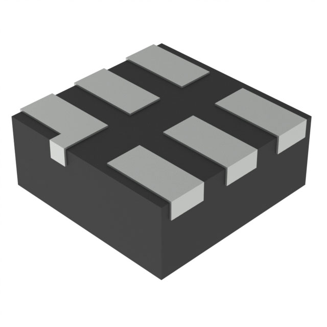
IC INVERT SCHMITT 2CH 2-INP 6SON
Datasheet:
Delivery:


Payment:


In Stock : 0
Please send RFQ , we will respond immediately.


SN74AUP2G14DSF2 Specifications
-
TypeParameter
-
Package / Case6-XFDFN
-
Supplier Device Package6-SON (1x1)
-
Mounting TypeSurface Mount
-
Operating Temperature-40°C ~ 85°C
-
Max Propagation Delay @ V, Max CL6.2ns @ 3.3V, 30pF
-
Input Logic Level - High0.6V ~ 2.29V
-
Input Logic Level - Low0.1V ~ 0.88V
-
Current - Output High, Low4mA, 4mA
-
Current - Quiescent (Max)500 nA
-
Voltage - Supply0.8V ~ 3.6V
-
FeaturesSchmitt Trigger
-
Number of Inputs2
-
Number of Circuits2
-
Logic TypeInverter
-
PackagingCut Tape (CT)
-
PackagingTape & Reel (TR)
-
Product StatusActive
-
Series74AUP
The SN74AUP2G14DSF2 is a dual Schmitt-trigger inverter integrated circuit chip. It offers several advantages and can be used in various application scenarios. Some of the advantages and application scenarios of this chip are:Advantages: 1. Low power consumption: The SN74AUP2G14DSF2 operates at a low power supply voltage, making it suitable for battery-powered devices and low-power applications. 2. High-speed operation: It has a high-speed propagation delay, enabling it to perform fast switching operations. 3. Schmitt-trigger input: The Schmitt-trigger input allows the chip to have hysteresis, making it less susceptible to noise and providing better noise immunity. 4. Wide operating voltage range: It can operate over a wide voltage range, making it compatible with various voltage levels.Application Scenarios: 1. Signal conditioning: The Schmitt-trigger input of the SN74AUP2G14DSF2 makes it suitable for signal conditioning applications. It can be used to clean up noisy signals and provide stable output signals. 2. Oscillators and clock generation: The high-speed operation of the chip makes it suitable for generating clock signals and building oscillators in digital systems. 3. Level shifting: The wide operating voltage range of the chip allows it to be used for level shifting applications, where signals need to be converted from one voltage level to another. 4. Logic gates: The SN74AUP2G14DSF2 can be used as a basic building block for implementing various logic functions in digital circuits, such as AND, OR, and NOT gates.Overall, the SN74AUP2G14DSF2 integrated circuit chip offers low power consumption, high-speed operation, noise immunity, and wide voltage range, making it suitable for a range of applications in signal conditioning, clock generation, level shifting, and logic gate implementation.
SN74AUP2G14DSF2 Relevant information
