


Share

SN74AUP2G14DSFR
Manufacturer No:
SN74AUP2G14DSFR
Manufacturer:
Description:
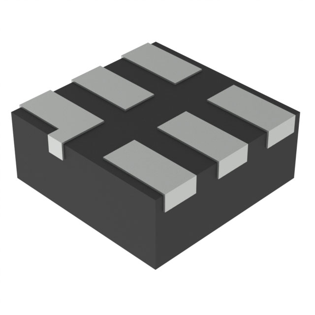
IC INVERT SCHMITT 2CH 2-INP 6SON
Datasheet:
Delivery:


Payment:


In Stock : 0
Please send RFQ , we will respond immediately.


SN74AUP2G14DSFR Specifications
-
TypeParameter
-
Package / Case6-XFDFN
-
Supplier Device Package6-SON (1x1)
-
Mounting TypeSurface Mount
-
Operating Temperature-40°C ~ 85°C
-
Max Propagation Delay @ V, Max CL6.2ns @ 3.3V, 30pF
-
Input Logic Level - High0.6V ~ 2.29V
-
Input Logic Level - Low0.1V ~ 0.88V
-
Current - Output High, Low4mA, 4mA
-
Current - Quiescent (Max)500 nA
-
Voltage - Supply0.8V ~ 3.6V
-
FeaturesSchmitt Trigger
-
Number of Inputs2
-
Number of Circuits2
-
Logic TypeInverter
-
PackagingCut Tape (CT)
-
PackagingTape & Reel (TR)
-
Product StatusActive
-
Series74AUP
The SN74AUP2G14DSFR is a specific model of integrated circuit chip manufactured by Texas Instruments. It is a dual Schmitt-trigger inverter, which means it has two independent inverters with Schmitt-trigger inputs. Here are some advantages and application scenarios of this chip:Advantages: 1. Low power consumption: The SN74AUP2G14DSFR is designed to operate at very low power levels, making it suitable for battery-powered devices and energy-efficient applications. 2. Wide operating voltage range: It can operate within a wide voltage range, typically from 0.8V to 3.6V, allowing compatibility with various voltage levels. 3. Schmitt-trigger inputs: The Schmitt-trigger inputs provide hysteresis, which helps in reducing noise and improving the noise immunity of the circuit. 4. Small form factor: The chip is available in a small package, such as the 6-ball wafer chip scale package (WCSP), making it suitable for space-constrained applications.Application scenarios: 1. Signal conditioning: The Schmitt-trigger inputs of the SN74AUP2G14DSFR make it useful for signal conditioning applications, where it can clean up noisy or distorted signals. 2. Level shifting: The wide operating voltage range of the chip allows it to be used for level shifting applications, where it can convert signals from one voltage level to another. 3. Oscillators and clock generation: The inverters in the chip can be used to build oscillators and clock generation circuits, providing stable and accurate timing signals. 4. Logic gates: The inverters can be used as basic building blocks for various logic functions, such as AND, OR, and NAND gates, enabling the implementation of digital logic circuits.It's important to note that the specific advantages and application scenarios may vary depending on the requirements and design considerations of a particular project.
SN74AUP2G14DSFR Relevant information
