


Share

74LVC2G06FW4-7
Manufacturer No:
74LVC2G06FW4-7
Manufacturer:
Description:
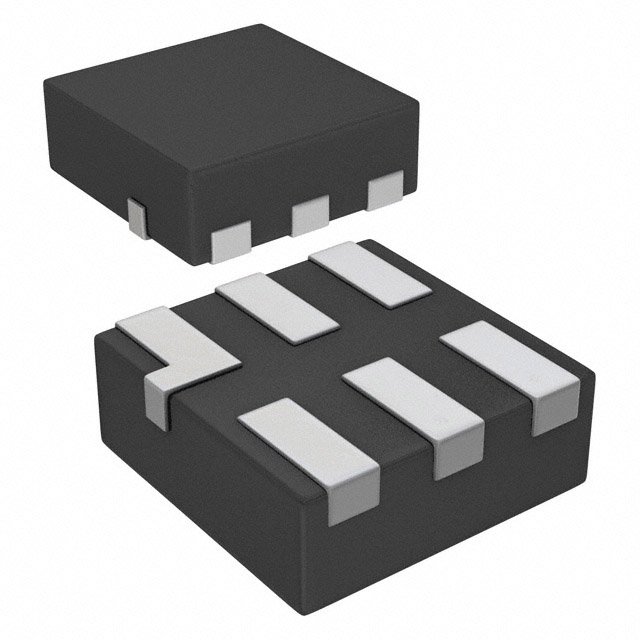
IC INVERT OD 2CH 2-INP DFN1010-6
Datasheet:
Delivery:


Payment:


In Stock : 0
Please send RFQ , we will respond immediately.


74LVC2G06FW4-7 Specifications
-
TypeParameter
-
Package / Case6-XFDFN
-
Supplier Device PackageX2-DFN1010-6
-
Mounting TypeSurface Mount
-
Operating Temperature-40°C ~ 125°C
-
Max Propagation Delay @ V, Max CL2.9ns @ 5V, 50pF
-
Input Logic Level - High1.7V ~ 2V
-
Input Logic Level - Low0.7V ~ 0.8V
-
Current - Output High, Low-, 32mA
-
Current - Quiescent (Max)10 µA
-
Voltage - Supply1.65V ~ 5.5V
-
FeaturesOpen Drain
-
Number of Inputs2
-
Number of Circuits2
-
Logic TypeInverter
-
PackagingTape & Reel (TR)
-
Product StatusActive
-
Series74LVC
The 74LVC2G06FW4-7 is a dual inverter buffer with open-drain outputs integrated circuit chip. Some of its advantages and application scenarios include:Advantages: 1. Low power consumption: The chip operates at a low voltage and consumes minimal power, making it suitable for battery-powered devices and energy-efficient applications. 2. Wide operating voltage range: It can operate within a wide voltage range, typically from 1.65V to 5.5V, allowing compatibility with various logic levels. 3. High-speed operation: The chip has a high-speed propagation delay, enabling fast signal processing and data transmission. 4. Open-drain outputs: The open-drain outputs provide flexibility in connecting to other devices, allowing for wired-OR configurations and multi-voltage level interfacing. 5. Small form factor: The chip is available in a small package, making it suitable for space-constrained applications and compact designs.Application scenarios: 1. Level shifting: The 74LVC2G06FW4-7 can be used to shift logic levels between different voltage domains, enabling communication between devices operating at different voltage levels. 2. Bus buffering: It can be used to buffer and drive signals on a bus, ensuring signal integrity and preventing signal degradation in multi-device communication systems. 3. Wired-OR configurations: The open-drain outputs of the chip make it suitable for implementing wired-OR logic, where multiple devices can drive a common signal line without conflicts. 4. I2C and SMBus applications: The chip can be used in I2C (Inter-Integrated Circuit) and SMBus (System Management Bus) applications for level shifting and signal buffering. 5. Battery-powered devices: Due to its low power consumption, the chip is suitable for use in battery-powered devices such as portable electronics, wearables, and IoT devices.It is important to note that the specific application scenarios may vary depending on the requirements and design considerations of the overall system.
74LVC2G06FW4-7 Relevant information
