


Share

74LVC2G06GW-Q100H
Manufacturer No:
74LVC2G06GW-Q100H
Manufacturer:
Description:
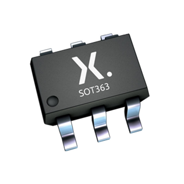
IC INVERTER OD 2CH 2-INP 6TSSOP
Datasheet:
Delivery:


Payment:


In Stock : 0
Please send RFQ , we will respond immediately.


74LVC2G06GW-Q100H Specifications
-
TypeParameter
-
Package / Case6-TSSOP, SC-88, SOT-363
-
Supplier Device Package6-TSSOP
-
Mounting TypeSurface Mount
-
Operating Temperature-40°C ~ 125°C
-
Max Propagation Delay @ V, Max CL2.9ns @ 5V, 50pF
-
Input Logic Level - High1.7V ~ 2V
-
Input Logic Level - Low0.7V ~ 0.8V
-
Current - Output High, Low-, 32mA
-
Current - Quiescent (Max)4 µA
-
Voltage - Supply1.65V ~ 5.5V
-
FeaturesOpen Drain
-
Number of Inputs2
-
Number of Circuits2
-
Logic TypeInverter
-
PackagingCut Tape (CT)
-
PackagingTape & Reel (TR)
-
Product StatusActive
-
SeriesAutomotive, AEC-Q100, 74LVC
The 74LVC2G06GW-Q100H is a dual inverter gate integrated circuit chip. It is part of the 74LVC series, which is a family of low-voltage CMOS logic chips. Here are some advantages and application scenarios of the 74LVC2G06GW-Q100H:Advantages: 1. Low-voltage operation: The chip operates at a low voltage range of 1.65V to 5.5V, making it suitable for battery-powered devices and low-power applications. 2. High-speed operation: It has a high-speed propagation delay, allowing for fast switching and signal processing. 3. Low power consumption: The chip is designed to consume minimal power, making it energy-efficient. 4. Wide operating temperature range: It can operate in a wide temperature range of -40°C to 125°C, making it suitable for various environments.Application scenarios: 1. Signal inversion: The 74LVC2G06GW-Q100H is commonly used for signal inversion applications, where it takes an input signal and produces its complement as the output. 2. Logic level shifting: It can be used to shift logic levels between different voltage domains, allowing for compatibility between devices operating at different voltage levels. 3. Buffering: The chip can be used as a buffer to isolate and amplify signals, ensuring proper signal integrity and driving capability. 4. Clock signal generation: It can be used to generate clock signals with precise timing and low jitter, making it suitable for clocking applications in digital systems. 5. Voltage level translation: The chip can be used to translate signals between different voltage levels, enabling communication between devices with different voltage requirements.Overall, the 74LVC2G06GW-Q100H is a versatile integrated circuit chip that finds applications in various digital systems, including consumer electronics, industrial automation, automotive electronics, and more.
74LVC2G06GW-Q100H Relevant information
