


Share

74LVC1G04FW5-7
Manufacturer No:
74LVC1G04FW5-7
Manufacturer:
Description:
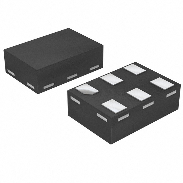
IC INVERTER 1CH 1-INP DFN1010-6
Datasheet:
Delivery:


Payment:


In Stock : 0
Please send RFQ , we will respond immediately.


74LVC1G04FW5-7 Specifications
-
TypeParameter
-
Package / Case6-XFDFN
-
Supplier Device PackageX1-DFN1010-6
-
Mounting TypeSurface Mount
-
Operating Temperature-40°C ~ 125°C (TA)
-
Max Propagation Delay @ V, Max CL5ns @ 5V, 50pF
-
Input Logic Level - High1.07V ~ 3.85V
-
Input Logic Level - Low0.58V ~ 1.65V
-
Current - Output High, Low32mA, 32mA
-
Current - Quiescent (Max)10 µA
-
Voltage - Supply1.65V ~ 5.5V
-
Features-
-
Number of Inputs1
-
Number of Circuits1
-
Logic TypeInverter
-
PackagingCut Tape (CT)
-
PackagingTape & Reel (TR)
-
Product StatusActive
-
Series74LVC
The 74LVC1G04FW5-7 (or 74LVC1G04) is a single inverter gate integrated circuit chip from NXP Semiconductors. It is part of the LVC (Low Voltage CMOS) logic family and is designed to operate at a power supply voltage of 1.65V to 5.5V. Some advantages and application scenarios of this chip are:Advantages: 1. Low power consumption: The 74LVC1G04 operates at lower power levels compared to other families, making it suitable for battery-powered devices or low-power applications. 2. Wide operating voltage range: With a supply voltage range of 1.65V to 5.5V, it can be used in various systems operating at different supply voltages. 3. High-speed operation: The 74LVC1G04 supports high-speed signal switching, making it suitable for applications where fast response times are required. 4. Compact package: The chip is available in a small surface-mount package, enabling it to be used in space-constrained designs.Application Scenarios: 1. Signal level conversion: The 74LVC1G04 can be used to convert logic signal levels from one voltage range to another. For example, it can interface between a microcontroller operating at 3.3V and a peripheral device requiring 5V logic levels. 2. Clock signal buffering: It can be used to buffer and invert clock signals in digital systems, ensuring proper signal integrity and synchronization. 3. Logic gate building blocks: The 74LVC1G04 can serve as a building block for designing various logic circuits such as oscillators, delay lines, and gates with different logical functions (e.g., AND, OR, XOR). 4. Voltage level shifters: It can act as a bidirectional level shifter, converting logic signals between different voltage domains, which is particularly useful when interfacing modules or devices operating at different supply voltages. 5. General-purpose inverter: The chip can be used as a simple inverter to complement logical operation in various digital circuits.These are just a few examples of the advantages and application scenarios for the 74LVC1G04FW5-7 integrated circuit chip. Its compact size, low power consumption, wide operating voltage range, and high-speed operation make it a versatile component in digital system designs.
74LVC1G04FW5-7 Relevant information
