


Share

74AUP1G06GW-Q100H
Manufacturer No:
74AUP1G06GW-Q100H
Manufacturer:
Description:
IC INVERTER OD 1CH 1-INP 5TSSOP
Datasheet:
Delivery:


Payment:


In Stock : 0
Please send RFQ , we will respond immediately.


74AUP1G06GW-Q100H Specifications
-
TypeParameter
-
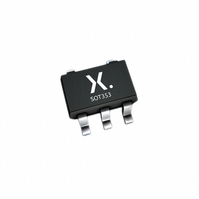
Package / Case5-TSSOP, SC-70-5, SOT-353
-
Supplier Device Package5-TSSOP
-
Mounting TypeSurface Mount
-
Operating Temperature-40°C ~ 125°C
-
Max Propagation Delay @ V, Max CL10.5ns @ 3.3V, 30pF
-
Input Logic Level - High1.6V ~ 2V
-
Input Logic Level - Low0.7V ~ 0.9V
-
Current - Output High, Low-, 4mA
-
Current - Quiescent (Max)500 nA
-
Voltage - Supply0.8V ~ 3.6V
-
FeaturesOpen Drain
-
Number of Inputs1
-
Number of Circuits1
-
Logic TypeInverter
-
PackagingCut Tape (CT)
-
PackagingTape & Reel (TR)
-
Product StatusActive
-
SeriesAutomotive, AEC-Q100, 74AUP
The 74AUP1G06GW-Q100H is a single inverter gate integrated circuit chip. It belongs to the 74AUP1G logic family, which is designed for low-power applications. Here are some advantages and application scenarios of this chip:Advantages: 1. Low power consumption: The 74AUP1G06GW-Q100H operates at a low supply voltage (1.0V to 3.6V) and consumes very low power, making it suitable for battery-powered devices and energy-efficient applications. 2. High-speed operation: This chip offers high-speed operation with propagation delays as low as 2.5ns, enabling fast signal processing and data transmission. 3. Wide operating temperature range: The 74AUP1G06GW-Q100H is designed to operate in a wide temperature range (-40°C to 125°C), making it suitable for various industrial and automotive applications.Application scenarios: 1. Signal level shifting: The 74AUP1G06GW-Q100H can be used to shift the logic levels of signals between different voltage domains. It can convert a high-level signal to a low-level signal or vice versa, enabling compatibility between different logic families or voltage levels. 2. Buffering and signal inversion: This chip can be used as a buffer to amplify and stabilize weak input signals. It can also invert the logic level of a signal, converting a high-level input to a low-level output or vice versa. 3. Clock signal generation: The 74AUP1G06GW-Q100H can be used to generate clock signals with precise timing characteristics. It can produce stable and accurate clock signals for various digital systems and applications. 4. Logic gate implementation: This chip can be used to implement basic logic functions like NOT gates or inverters. It can be combined with other logic gates to build more complex digital circuits and systems.Overall, the 74AUP1G06GW-Q100H integrated circuit chip offers low power consumption, high-speed operation, and wide temperature range, making it suitable for various low-power and high-performance applications in industries such as automotive, industrial automation, consumer electronics, and telecommunications.
74AUP1G06GW-Q100H Relevant information
