


Share

74AUP1G14FS3-7
Manufacturer No:
74AUP1G14FS3-7
Manufacturer:
Description:
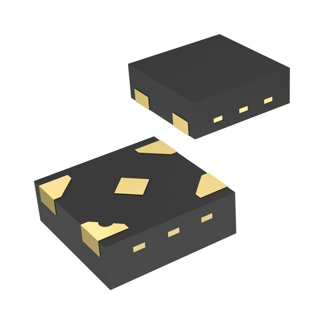
IC INVERTER 1CH 1-INP DFN0808-4
Datasheet:
Delivery:


Payment:


In Stock : 0
Please send RFQ , we will respond immediately.


74AUP1G14FS3-7 Specifications
-
TypeParameter
-
Package / Case4-XFDFN Exposed Pad
-
Supplier Device PackageX2-DFN0808-4
-
Mounting TypeSurface Mount
-
Operating Temperature-40°C ~ 125°C
-
Max Propagation Delay @ V, Max CL6.1ns @ 3.3V, 30pF
-
Input Logic Level - High0.65V ~ 2.32V
-
Input Logic Level - Low0.15V ~ 0.88V
-
Current - Output High, Low4mA, 4mA
-
Current - Quiescent (Max)500 nA
-
Voltage - Supply0.8V ~ 3.6V
-
FeaturesSchmitt Trigger
-
Number of Inputs1
-
Number of Circuits1
-
Logic TypeInverter
-
PackagingTape & Reel (TR)
-
Product StatusActive
-
Series74AUP
The 74AUP1G14FS3-7 is a single inverter gate integrated circuit chip. Some of its advantages and application scenarios are as follows:Advantages: 1. Low power consumption: The 74AUP1G14FS3-7 operates at a low supply voltage (1.0V to 3.6V) and consumes very low power, making it suitable for battery-powered devices and low-power applications. 2. High-speed operation: It has a high-speed propagation delay of 2.5 ns (typical) at 3.3V supply voltage, enabling fast signal processing. 3. Small form factor: The chip is available in a small SOT353 package, which makes it suitable for space-constrained applications and miniaturized designs. 4. Wide operating temperature range: It can operate in a temperature range of -40°C to +125°C, making it suitable for various environmental conditions.Application scenarios: 1. Logic level conversion: The 74AUP1G14FS3-7 can be used to convert logic levels between different voltage domains. For example, it can be used to interface a microcontroller operating at 3.3V with a peripheral device operating at 1.8V. 2. Signal buffering: It can be used to buffer and amplify weak signals, ensuring proper signal integrity and preventing signal degradation. 3. Clock signal generation: The chip can be used to generate clock signals with precise timing characteristics, which are essential in digital systems and communication protocols. 4. Waveform shaping: It can be used to shape and modify digital waveforms, such as generating square waves or pulse signals with specific characteristics. 5. Voltage level detection: The chip can be used to detect voltage levels and generate corresponding digital outputs, enabling voltage monitoring and threshold detection applications.Overall, the 74AUP1G14FS3-7 integrated circuit chip offers low power consumption, high-speed operation, and small form factor, making it suitable for a wide range of applications in various industries, including consumer electronics, automotive, industrial automation, and telecommunications.
74AUP1G14FS3-7 Relevant information
