


Share

SN74AS804BDW
Manufacturer No:
SN74AS804BDW
Manufacturer:
Description:
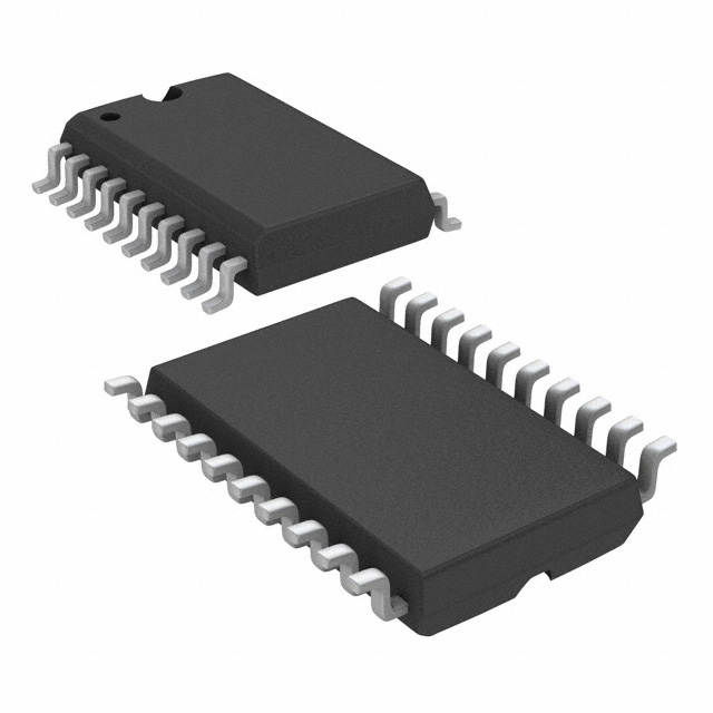
IC GATE NAND 6CH 2-INP 20SOIC
Datasheet:
Delivery:


Payment:


In Stock : 2
Please send RFQ , we will respond immediately.


SN74AS804BDW Specifications
-
TypeParameter
-
Package / Case20-SOIC (0.295", 7.50mm Width)
-
Supplier Device Package20-SOIC
-
Mounting TypeSurface Mount
-
Operating Temperature0°C ~ 70°C
-
Max Propagation Delay @ V, Max CL4ns @ 5V, 50pF
-
Input Logic Level - High2V
-
Input Logic Level - Low0.8V
-
Current - Output High, Low48mA, 48mA
-
Current - Quiescent (Max)-
-
Voltage - Supply4.5V ~ 5.5V
-
Features-
-
Number of Inputs2
-
Number of Circuits6
-
Logic TypeNAND Gate
-
PackagingTube
-
PackagingBulk
-
Product StatusActive
-
Series74AS
The SN74AS804BDW is a 9-bit addressable latch integrated circuit chip. Some of the advantages and application scenarios of this chip are as follows:Advantages: 1. High Speed: The SN74AS804BDW operates at a high-speed operation with a typical propagation delay of 5.5 ns, enabling quick data transfers and efficient processing.2. Addressable Latches: This chip consists of 9 addressable latches, allowing each latch to be individually controlled. This feature provides flexibility in data storage and retrieval operations.3. Compatibility: The SN74AS804BDW is designed to be compatible with other TTL (Transistor-Transistor Logic) families, making it able to interface with various other digital logic circuits and systems.4. Output Enable Function: It includes an active-low output enable (OE) pin that helps control the output states of the latches, contributing to efficient power management and data handling.Application Scenarios: 1. Address Decoding: The SN74AS804BDW can be used in address decoding applications such as memory interfacing and memory mapping, where it enables the selection of specific memory locations based on the input address.2. Data Storage: With its 9 addressable latches, this chip can be utilized for data storage applications that require efficient and controlled storage of binary information.3. Register Design: The chip's latches can be used to build various types of registers, such as shift registers or parallel-in-serial-out (PISO) registers, providing flexibility for data manipulation and transfer.4. System Control: The SN74AS804BDW can serve as a component in system control circuits, where it plays a role in controlling the flow of data or state transitions based on specific address inputs.Overall, the SN74AS804BDW integrated circuit chip offers high-speed operation, addressable latch functionality, compatibility with TTL families, and output enable capability, making it suitable for various applications requiring efficient data storage, control, and interfacing.
SN74AS804BDW Relevant information
