


Share

CD4049UBNSR
Manufacturer No:
CD4049UBNSR
Manufacturer:
Description:
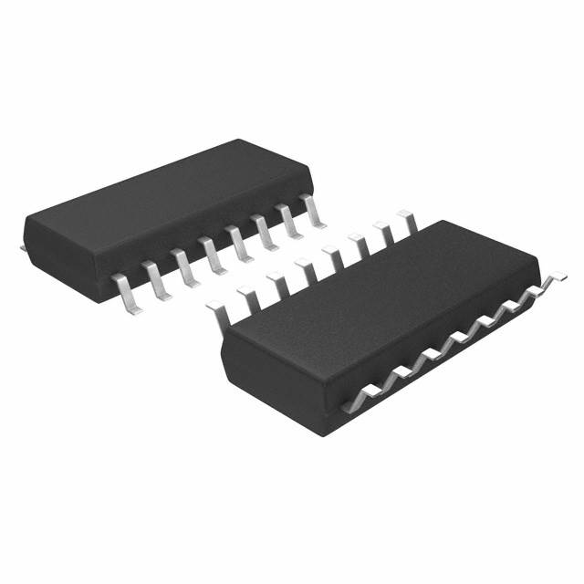
IC INVERTER 6CH 1-INP 16SO
Datasheet:
Delivery:


Payment:


In Stock : 418
Please send RFQ , we will respond immediately.


CD4049UBNSR Specifications
-
TypeParameter
-
Package / Case16-SOIC (0.209", 5.30mm Width)
-
Supplier Device Package16-SO
-
Mounting TypeSurface Mount
-
Operating Temperature-55°C ~ 125°C
-
Max Propagation Delay @ V, Max CL50ns @ 15V, 50pF
-
Input Logic Level - High4V ~ 12.5V
-
Input Logic Level - Low1V ~ 2.5V
-
Current - Output High, Low4.3mA, 24mA
-
Current - Quiescent (Max)4 µA
-
Voltage - Supply3V ~ 18V
-
Features-
-
Number of Inputs1
-
Number of Circuits6
-
Logic TypeInverter
-
PackagingCut Tape (CT)
-
PackagingTape & Reel (TR)
-
Product StatusActive
-
Series4000B
The CD4049UBNSR is a hex inverter integrated circuit chip. It has several advantages and application scenarios, including:1. Wide voltage range: The CD4049UBNSR operates over a wide voltage range, typically from 3V to 18V. This makes it suitable for various applications and compatible with different power supply voltages.2. High noise immunity: It has a high noise immunity, which means it can tolerate noise and interference in the input signals without affecting the output. This makes it reliable in noisy environments.3. Low power consumption: The CD4049UBNSR is designed to consume low power, making it suitable for battery-powered devices or applications where power efficiency is crucial.4. Compact and versatile: The chip is available in a small package, making it easy to integrate into various electronic circuits. It can be used in a wide range of applications, including signal processing, voltage level shifting, waveform generation, and logic gate interfacing.5. Inverter functionality: The CD4049UBNSR consists of six independent inverters, which can be used to invert the logic level of input signals. This makes it useful in applications where logic inversion is required, such as in digital systems, microcontrollers, and communication circuits.6. Signal buffering: The chip can be used as a buffer to isolate different sections of a circuit, preventing interference between them. It helps in maintaining signal integrity and preventing signal degradation.Application scenarios for CD4049UBNSR include:1. Logic level shifting: The chip can be used to shift the logic levels of signals from one voltage domain to another. This is useful when interfacing different logic families or devices with different voltage requirements.2. Oscillator and waveform generation: The inverters in the CD4049UBNSR can be used to create oscillators and generate different waveforms, such as square waves or pulse signals. This is useful in applications like clock generation, timing circuits, and frequency modulation.3. Signal conditioning: The chip can be used to condition or modify input signals before further processing. It can be used to invert, amplify, or buffer signals to match the requirements of downstream components.4. Noise filtering: The high noise immunity of the CD4049UBNSR makes it suitable for applications where noise filtering is required. It can be used to clean up noisy signals and improve signal quality.5. Logic gate interfacing: The chip can be used to interface different logic gates or logic families. It can convert signals from one logic level to another, ensuring compatibility between different components or systems.Overall, the CD4049UBNSR is a versatile and reliable integrated circuit chip with various advantages and can be applied in a wide range of electronic circuits and systems.
CD4049UBNSR Relevant information
