


Share

SN74AUP1G04DSF2
Manufacturer No:
SN74AUP1G04DSF2
Manufacturer:
Description:
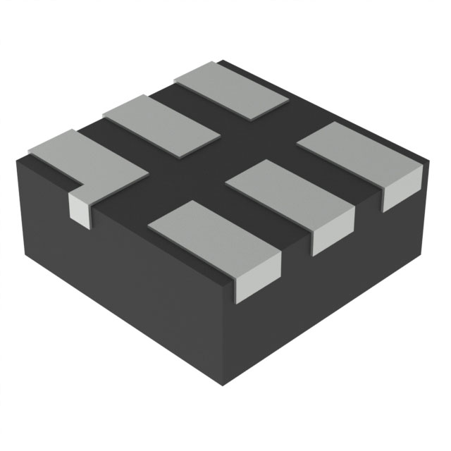
IC INVERTER 1CH 1-INP 6SON
Datasheet:
Delivery:


Payment:


In Stock : 661
Please send RFQ , we will respond immediately.


SN74AUP1G04DSF2 Specifications
-
TypeParameter
-
Package / Case6-XFDFN
-
Supplier Device Package6-SON (1x1)
-
Mounting TypeSurface Mount
-
Operating Temperature-40°C ~ 85°C
-
Max Propagation Delay @ V, Max CL5.4ns @ 3.3V, 30pF
-
Input Logic Level - High1.6V ~ 2V
-
Input Logic Level - Low0.7V ~ 0.9V
-
Current - Output High, Low4mA, 4mA
-
Current - Quiescent (Max)500 nA
-
Voltage - Supply0.8V ~ 3.6V
-
Features-
-
Number of Inputs1
-
Number of Circuits1
-
Logic TypeInverter
-
PackagingCut Tape (CT)
-
PackagingTape & Reel (TR)
-
Product StatusActive
-
Series74AUP
The SN74AUP1G04DSF2 is a single inverter gate integrated circuit chip manufactured by Texas Instruments. It is part of the AUP family of devices, which are designed for low-power applications. Here are some advantages and application scenarios of the SN74AUP1G04DSF2:Advantages: 1. Low power consumption: The AUP family of devices is optimized for low-power operation, making it suitable for battery-powered applications or any scenario where power efficiency is crucial. 2. Wide operating voltage range: The SN74AUP1G04DSF2 can operate within a wide voltage range, typically from 0.8V to 3.6V. This flexibility allows it to be used in various voltage domains or mixed-voltage level applications. 3. High-speed operation: The chip has a high-speed propagation delay, enabling it to process signals quickly and efficiently. 4. Small form factor: The SN74AUP1G04DSF2 is available in a small package, such as the 5-pin SC-70 (DFN) package, which makes it suitable for space-constrained designs.Application Scenarios: 1. Battery-powered devices: Due to its low power consumption, the SN74AUP1G04DSF2 is ideal for use in portable or battery-powered devices, such as smartphones, tablets, wearables, or IoT devices. 2. Level shifting: The wide operating voltage range of the chip makes it suitable for level shifting applications, where signals need to be converted between different voltage domains. 3. Signal buffering: The high-speed operation of the SN74AUP1G04DSF2 makes it suitable for buffering or amplifying signals in various digital systems, such as microcontrollers, FPGAs, or communication interfaces. 4. General-purpose logic: The chip can be used as a general-purpose logic gate, providing signal inversion functionality in various digital circuits.It is important to note that the specific advantages and application scenarios may vary depending on the requirements of the project and the overall system design. It is recommended to consult the datasheet and application notes provided by Texas Instruments for detailed information and guidelines on using the SN74AUP1G04DSF2 in specific applications.
SN74AUP1G04DSF2 Relevant information
