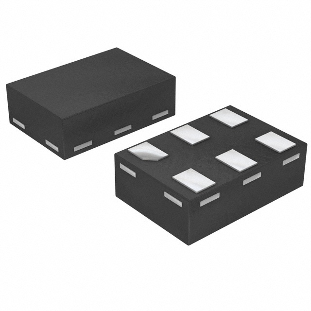
74LVC1G00FW5-7
Manufacturer No:
74LVC1G00FW5-7
Manufacturer:
Description:
IC GATE NAND 1CH 2-INP DFN1010-6
Datasheet:
Delivery:


Payment:


In Stock : 410
Please send RFQ , we will respond immediately.


74LVC1G00FW5-7 Specifications
-
TypeParameter
-
Package / Case6-XFDFN
-
Supplier Device PackageX1-DFN1010-6
-
Mounting TypeSurface Mount
-
Operating Temperature-40°C ~ 125°C
-
Max Propagation Delay @ V, Max CL5.5ns @ 5V, 50pF
-
Input Logic Level - High1.7V ~ 2V
-
Input Logic Level - Low0.7V ~ 0.8V
-
Current - Output High, Low32mA, 32mA
-
Current - Quiescent (Max)200 µA
-
Voltage - Supply1.65V ~ 5.5V
-
Features-
-
Number of Inputs2
-
Number of Circuits1
-
Logic TypeNAND Gate
-
PackagingCut Tape (CT)
-
PackagingTape & Reel (TR)
-
Product StatusActive
-
Series74LVC
The 74LVC1G00FW5-7 integrated circuit chip is a single 2-input NAND gate chip. Some advantages and application scenarios of this chip are:Advantages: 1. Small Package Size: The chip is available in a small SOT353 package, making it suitable for compact designs and space-constrained applications. 2. Low Power Consumption: It operates on low power supply voltage, typically ranging from 1.65V to 5.5V. This makes it ideal for battery-powered devices or applications that require efficient power management. 3. High-Speed Operation: The chip is designed to operate at high speeds, enabling rapid data processing and signal transmission. 4. Wide Operating Temperature Range: It can withstand a wide range of operating temperatures, typically from -40°C to +125°C. This makes it suitable for various industrial and automotive applications.Application Scenarios: 1. Logic Gates: The 74LVC1G00FW5-7 chip can be used to implement basic logic functions in digital systems, such as inverting, buffering, and signal routing. It can be employed as a building block for various logic operations in microcontrollers, FPGA-based systems, or digital circuits. 2. Signal Processing: It can be used in applications that require signal conditioning, waveform generation, or noise filtering. The NAND gate functionality of the chip allows for logical operations on signals, making it useful in data processing and control systems. 3. Level Shifting: It can be utilized to convert voltage levels between different logic families or to interface between circuits operating at different voltage levels. The chip's compatibility with different power supply voltages makes it suitable for level shifting applications in mixed voltage systems. 4. Clock and Timing Applications: The chip can be used in clock distribution, clock gating, or clock signal generation circuits. It enables synchronization and control of timing sequences in digital systems.Please note that the specific use cases of the chip may vary depending on the requirements of the system and the designer's creativity.
74LVC1G00FW5-7 Relevant information


