


Share

CD4025BMT
Manufacturer No:
CD4025BMT
Manufacturer:
Description:
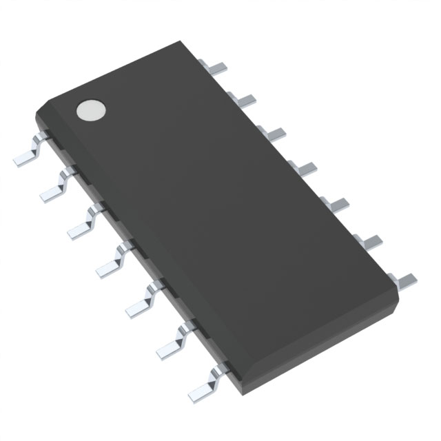
IC GATE NOR 3CH 3-INP 14SOIC
Datasheet:
Delivery:


Payment:


In Stock : 1077
Please send RFQ , we will respond immediately.


CD4025BMT Specifications
-
TypeParameter
-
Package / Case14-SOIC (0.154", 3.90mm Width)
-
Supplier Device Package14-SOIC
-
Mounting TypeSurface Mount
-
Operating Temperature-55°C ~ 125°C
-
Max Propagation Delay @ V, Max CL90ns @ 15V, 50pF
-
Input Logic Level - High3.5V ~ 11V
-
Input Logic Level - Low1.5V ~ 4V
-
Current - Output High, Low3.4mA, 3.4mA
-
Current - Quiescent (Max)1 µA
-
Voltage - Supply3V ~ 18V
-
Features-
-
Number of Inputs3
-
Number of Circuits3
-
Logic TypeNOR Gate
-
PackagingCut Tape (CT)
-
PackagingTape & Reel (TR)
-
Product StatusLast Time Buy
-
Series4000B
The CD4025BMT is a CMOS integrated circuit chip that offers several advantages and can be used in various application scenarios. Some of the advantages and application scenarios of the CD4025BMT are:Advantages: 1. Low power consumption: The CD4025BMT operates at a low power supply voltage and consumes minimal power, making it suitable for battery-powered devices and low-power applications. 2. High noise immunity: The chip has a high noise immunity, which means it can tolerate external noise and interference, ensuring reliable operation in noisy environments. 3. Wide operating voltage range: The CD4025BMT can operate over a wide range of power supply voltages, making it versatile and compatible with different power sources. 4. Multiple inputs: The chip has three independent input gates, allowing multiple input signals to be processed simultaneously. 5. Schmitt trigger inputs: The CD4025BMT features Schmitt trigger inputs, which provide hysteresis and improve noise immunity, making it suitable for applications with noisy or unstable input signals.Application scenarios: 1. Logic level conversion: The CD4025BMT can be used to convert logic levels between different voltage domains. It can take input signals from one voltage level and provide output signals at a different voltage level, enabling compatibility between different logic families or devices. 2. Signal conditioning: The Schmitt trigger inputs of the CD4025BMT make it suitable for signal conditioning applications. It can be used to clean up noisy or distorted input signals, ensuring reliable and accurate signal processing. 3. Debouncing: The chip can be used for debouncing switches or buttons. It can eliminate the bouncing effect caused by mechanical switches, providing a clean and stable signal for further processing. 4. Frequency division: The CD4025BMT can be used as a frequency divider. By connecting the input signal to one of the gates and cascading multiple chips, it is possible to divide the input frequency by various factors, generating lower frequency output signals. 5. Oscillator circuits: The chip can be used to build simple oscillator circuits. By connecting the output of one gate to the input of another gate, a feedback loop can be created, resulting in an oscillating output signal.These are just a few examples of the advantages and application scenarios of the CD4025BMT integrated circuit chip. Its versatility, low power consumption, and noise immunity make it suitable for a wide range of digital logic and signal processing applications.
CD4025BMT Relevant information
