


Share

CD4049UBD
Manufacturer No:
CD4049UBD
Manufacturer:
Description:
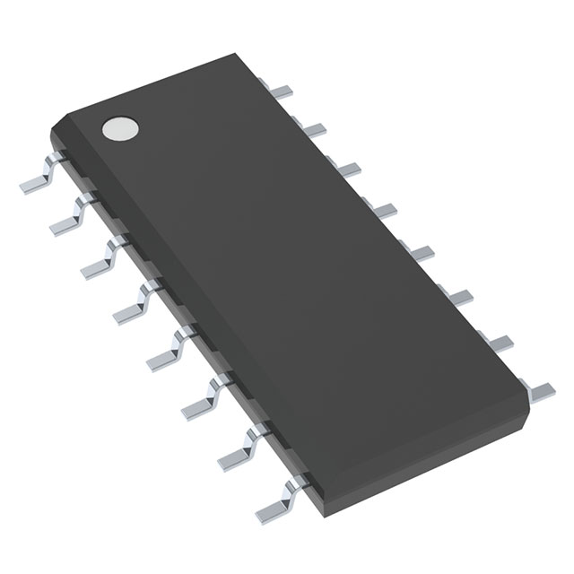
IC INVERTER 6CH 1-INP 16SOIC
Datasheet:
Delivery:


Payment:


In Stock : 1972
Please send RFQ , we will respond immediately.


CD4049UBD Specifications
-
TypeParameter
-
Package / Case16-SOIC (0.154", 3.90mm Width)
-
Supplier Device Package16-SOIC
-
Mounting TypeSurface Mount
-
Operating Temperature-55°C ~ 125°C
-
Max Propagation Delay @ V, Max CL50ns @ 15V, 50pF
-
Input Logic Level - High4V ~ 12.5V
-
Input Logic Level - Low1V ~ 2.5V
-
Current - Output High, Low4.3mA, 24mA
-
Current - Quiescent (Max)4 µA
-
Voltage - Supply3V ~ 18V
-
Features-
-
Number of Inputs1
-
Number of Circuits6
-
Logic TypeInverter
-
PackagingTube
-
Product StatusDiscontinued at Digi-Key
-
Series4000B
The CD4049UBD is a hex inverter/buffer integrated circuit chip. It offers several advantages and can be used in various application scenarios:Advantages: 1. Versatility: The CD4049UBD can be used as a hex inverter or a buffer, making it suitable for a wide range of applications. 2. High noise immunity: It has a high noise immunity, which means it can tolerate noise signals without affecting its performance. 3. Wide operating voltage range: The chip can operate within a wide voltage range, typically from 3V to 18V, making it compatible with different power supply configurations. 4. Low power consumption: It consumes low power, making it suitable for battery-powered devices or applications where power efficiency is crucial. 5. Compact size: The CD4049UBD is available in a small package, making it easy to integrate into various circuit designs.Application scenarios: 1. Signal inversion: The CD4049UBD can be used to invert digital signals. It is commonly used in applications where signal polarity needs to be reversed, such as in motor control circuits or data transmission systems. 2. Level shifting: It can be used to shift the voltage levels of digital signals. This is useful when interfacing between different logic families or when converting between different voltage levels. 3. Buffering: The CD4049UBD can be used as a buffer to isolate different sections of a circuit. It helps prevent loading effects and signal degradation when connecting different components together. 4. Oscillator circuits: The chip can be used to build simple oscillator circuits, generating square wave signals of different frequencies. These oscillators find applications in timing circuits, clock generation, or frequency modulation. 5. Logic gates: The CD4049UBD can be used to implement basic logic gates like AND, OR, NAND, NOR, XOR, and XNOR. These gates are building blocks for more complex digital circuits and can be used in various digital systems.Overall, the CD4049UBD offers versatility, noise immunity, and low power consumption, making it suitable for a wide range of applications in digital electronics.
CD4049UBD Relevant information
