


Share

SN74AUC1GU04DBVR
Manufacturer No:
SN74AUC1GU04DBVR
Manufacturer:
Description:
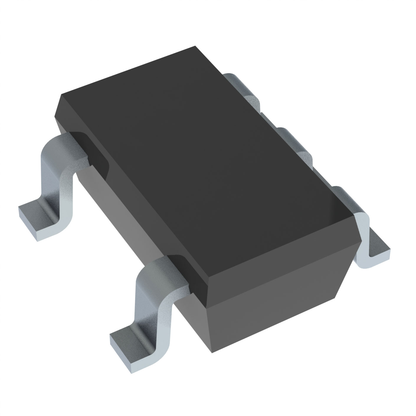
IC INVERTER 1CH 1-INP SOT23-5
Datasheet:
Delivery:


Payment:


In Stock : 5903
Please send RFQ , we will respond immediately.


SN74AUC1GU04DBVR Specifications
-
TypeParameter
-
Package / CaseSC-74A, SOT-753
-
Supplier Device PackageSOT-23-5
-
Mounting TypeSurface Mount
-
Operating Temperature-40°C ~ 85°C
-
Max Propagation Delay @ V, Max CL2.1ns @ 2.5V, 30pF
-
Input Logic Level - High-
-
Input Logic Level - Low-
-
Current - Output High, Low9mA, 9mA
-
Current - Quiescent (Max)10 µA
-
Voltage - Supply0.8V ~ 2.7V
-
Features-
-
Number of Inputs1
-
Number of Circuits1
-
Logic TypeInverter
-
PackagingCut Tape (CT)
-
PackagingTape & Reel (TR)
-
Product StatusActive
-
Series74AUC
The SN74AUC1GU04DBVR is a single inverter gate integrated circuit chip. It belongs to the AUC family of devices, which are part of the Texas Instruments' Advanced Ultra-Low Power CMOS logic family. Here are some advantages and application scenarios of the SN74AUC1GU04DBVR:Advantages: 1. Low power consumption: The AUC family of devices is designed for ultra-low power operation, making it suitable for battery-powered applications and energy-efficient designs. 2. Wide operating voltage range: The SN74AUC1GU04DBVR can operate over a wide voltage range, typically from 0.8V to 3.6V, allowing compatibility with various power supply levels. 3. High-speed operation: It offers fast switching speeds, enabling efficient signal processing and data transmission. 4. Small form factor: The chip comes in a small SOT-23 package, making it suitable for space-constrained designs and compact electronic devices.Application scenarios: 1. Battery-powered devices: The low power consumption of the SN74AUC1GU04DBVR makes it ideal for use in portable and battery-powered devices such as smartphones, tablets, wearables, and IoT devices. 2. Signal level shifting: The chip can be used for level shifting applications, where it converts signals from one voltage level to another, ensuring compatibility between different parts of a circuit. 3. Logic signal buffering: It can be used to buffer logic signals, ensuring signal integrity and preventing signal degradation in digital systems. 4. Clock signal generation: The SN74AUC1GU04DBVR can be used to generate clock signals in various digital systems, such as microcontrollers, FPGAs, and communication devices. 5. Voltage level conversion: It can be used to convert voltage levels between different logic families, allowing interfacing between devices with different voltage requirements.Overall, the SN74AUC1GU04DBVR integrated circuit chip offers low power consumption, high-speed operation, and small form factor, making it suitable for a wide range of applications in battery-powered devices, signal level shifting, logic buffering, clock signal generation, and voltage level conversion.
SN74AUC1GU04DBVR Relevant information
