


Share
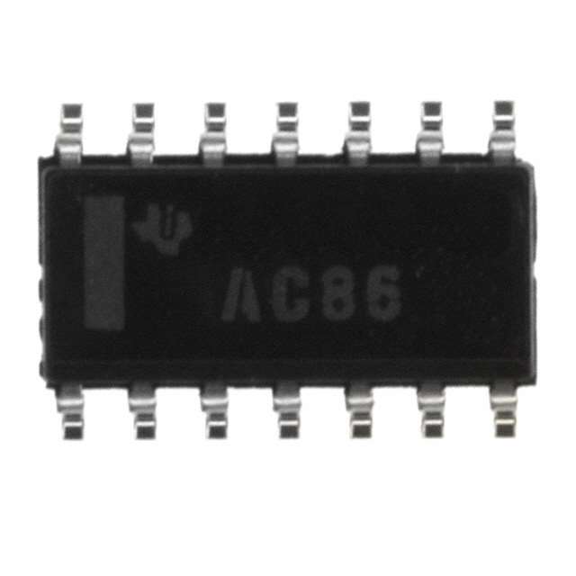

SN74LV06ADBR
Manufacturer No:
SN74LV06ADBR
Manufacturer:
Description:
IC INVERTER OD 6CH 1-INP 14SSOP
Datasheet:
Delivery:


Payment:


In Stock : 4730
Please send RFQ , we will respond immediately.


SN74LV06ADBR Specifications
-
TypeParameter
-
Package / Case14-SSOP (0.209", 5.30mm Width)
-
Supplier Device Package14-SSOP
-
Mounting TypeSurface Mount
-
Operating Temperature-40°C ~ 85°C
-
Max Propagation Delay @ V, Max CL7.5ns @ 5V, 50pF
-
Input Logic Level - High1.5V
-
Input Logic Level - Low0.5V
-
Current - Output High, Low-, 16mA
-
Current - Quiescent (Max)20 µA
-
Voltage - Supply2V ~ 5.5V
-
FeaturesOpen Drain
-
Number of Inputs1
-
Number of Circuits6
-
Logic TypeInverter
-
PackagingCut Tape (CT)
-
PackagingTape & Reel (TR)
-
Product StatusActive
-
Series74LV
The SN74LV06ADBR is a hex inverter buffer/driver with open-drain outputs. It is a type of integrated circuit chip that offers several advantages and can be used in various application scenarios. Some of the advantages and application scenarios of the SN74LV06ADBR are:Advantages: 1. Open-drain outputs: The open-drain outputs allow for easy interfacing with other devices, as they can be connected to external pull-up resistors to achieve different voltage levels. 2. Hex inverter buffer/driver: The chip provides six inverters, which can be used to invert logic signals or buffer them to drive other devices. 3. Low voltage operation: The SN74LV06ADBR operates at low voltage levels, typically between 1.65V and 5.5V, making it suitable for low-power applications. 4. Wide temperature range: The chip can operate over a wide temperature range, typically between -40°C and 125°C, making it suitable for various environments.Application Scenarios: 1. Level shifting: The open-drain outputs of the SN74LV06ADBR can be used for level shifting between different voltage domains. By connecting the outputs to external pull-up resistors, the chip can convert logic signals from one voltage level to another. 2. Bus buffering: The hex inverter buffer/driver functionality of the chip makes it suitable for buffering and driving signals on a bus. It can be used to amplify and transmit signals between different components in a system. 3. Logic inversion: The inverters provided by the chip can be used to invert logic signals. This is useful in applications where the polarity of a signal needs to be reversed. 4. I2C and SMBus applications: The open-drain outputs of the chip make it suitable for implementing the I2C (Inter-Integrated Circuit) and SMBus (System Management Bus) protocols, which use open-drain signaling.Overall, the SN74LV06ADBR integrated circuit chip offers the advantages of open-drain outputs, low voltage operation, and wide temperature range. It can be used in various application scenarios such as level shifting, bus buffering, logic inversion, and I2C/SMBus applications.
SN74LV06ADBR Relevant information
