


Share

SN74LV06APWR
Manufacturer No:
SN74LV06APWR
Manufacturer:
Description:
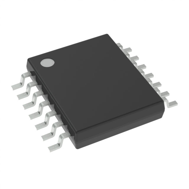
IC INVERTER OD 6CH 1-INP 14TSSOP
Datasheet:
Delivery:


Payment:


In Stock : 6114
Please send RFQ , we will respond immediately.


SN74LV06APWR Specifications
-
TypeParameter
-
Package / Case14-TSSOP (0.173", 4.40mm Width)
-
Supplier Device Package14-TSSOP
-
Mounting TypeSurface Mount
-
Operating Temperature-40°C ~ 85°C
-
Max Propagation Delay @ V, Max CL7.5ns @ 5V, 50pF
-
Input Logic Level - High1.5V
-
Input Logic Level - Low0.5V
-
Current - Output High, Low-, 16mA
-
Current - Quiescent (Max)20 µA
-
Voltage - Supply2V ~ 5.5V
-
FeaturesOpen Drain
-
Number of Inputs1
-
Number of Circuits6
-
Logic TypeInverter
-
PackagingCut Tape (CT)
-
PackagingTape & Reel (TR)
-
Product StatusActive
-
Series74LV
The SN74LV06APWR is a Hex Inverter Buffers/Drivers with Open-Drain Outputs integrated circuit chip. It offers several advantages and can be applied in various scenarios, including:Advantages: 1. High-speed operation: The SN74LV06APWR chip operates at a high switching speed, making it suitable for applications that require fast response times. 2. Low power consumption: It consumes low power, which is beneficial for battery-powered devices or applications where power efficiency is essential. 3. Open-drain outputs: The chip features open-drain outputs, which allow for flexible interfacing with other devices or circuits. Open-drain outputs can be easily pulled up or down externally, enabling them to be used in wired-OR or wired-AND configurations. 4. Wide voltage range compatibility: The SN74LV06APWR can operate within a wide voltage range, typically between 2V and 5.5V. This compatibility makes it suitable for various applications and interfacing with different voltage levels. 5. ESD protection: The chip is designed to provide Electrostatic Discharge (ESD) protection, safeguarding it against damage during handling or in environments with electrostatic discharge risks.Application Scenarios: 1. Level shifting and voltage translation: The SN74LV06APWR chip can be used to shift logic levels or translate voltages between different parts of a circuit, especially when interfacing devices with different voltage requirements. 2. Bus line buffering: It can be used to buffer bus lines, ensuring that signals are properly driven and received by the connected devices. The open-drain outputs enable easy wiring of multiple devices sharing a common bus line. 3. Pull-up/pull-down configurations: The chip's open-drain outputs can be utilized to implement pull-up or pull-down resistor networks and achieve wired-OR or wired-AND logic functionality. 4. General purpose digital logic: The SN74LV06APWR can be employed in a wide range of digital logic applications where simple logic functions such as inversion or buffering are required.It is important to note that the specific application and use case of the SN74LV06APWR may vary depending on the requirements and design of the circuit being implemented.
SN74LV06APWR Relevant information
