


Share

In Stock : 0
Please send RFQ , we will respond immediately.


NC7SVL04FHX Specifications
-
TypeParameter
-
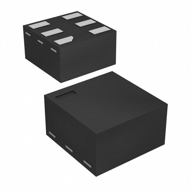
Mounting TypeSurface Mount
-
Operating Temperature-40°C ~ 85°C
-
Max Propagation Delay @ V, Max CL3.5ns @ 3V, 30pF
-
Input Logic Level - High0.9V ~ 1.5V
-
Input Logic Level - Low0.7V ~ 0.8V
-
Current - Output High, Low24mA, 24mA
-
Current - Quiescent (Max)900 nA
-
Voltage - Supply0.9V ~ 3.6V
-
Features-
-
Number of Inputs1
-
Number of Circuits1
-
Logic TypeInverter
-
PackagingTape & Reel (TR)
-
Product StatusObsolete
-
Series7SVL
The NC7SVL04FHX is a specific type of integrated circuit chip known as a hex inverter. It has six independent inverters, each capable of converting a logic level input signal into its complemented output signal. Here are some advantages and application scenarios of the NC7SVL04FHX chip:Advantages: 1. Small form factor: The chip is designed using advanced CMOS technology, allowing for a compact size and low power consumption. 2. Wide operating voltage range: It can operate within a wide voltage range, typically from 1.65V to 5.5V, making it compatible with various logic families. 3. High-speed operation: The chip offers fast switching speeds, enabling efficient signal processing in high-frequency applications. 4. Low power consumption: It consumes minimal power, making it suitable for battery-powered devices and energy-efficient applications. 5. ESD protection: The chip is equipped with built-in electrostatic discharge (ESD) protection, ensuring robustness against static electricity.Application scenarios: 1. Digital logic circuits: The NC7SVL04FHX chip can be used in various digital logic circuits, such as flip-flops, counters, and registers, to invert and manipulate logic signals. 2. Signal level shifting: It can be employed to convert logic levels between different voltage domains, enabling compatibility between devices operating at different voltage levels. 3. Clock signal inversion: In applications where an inverted clock signal is required, the hex inverter can be used to generate the complemented clock signal. 4. Buffering and line driving: The chip can be used to buffer and drive signals along transmission lines, ensuring signal integrity and preventing signal degradation. 5. Voltage level translation: It can be utilized to translate logic levels between different voltage standards, facilitating communication between devices with different voltage requirements.Overall, the NC7SVL04FHX chip's small size, low power consumption, and high-speed operation make it suitable for a wide range of digital logic applications, signal processing, and voltage level conversion scenarios.
NC7SVL04FHX Relevant information
