


Share

74LVC1G08GW/DG,125
Manufacturer No:
74LVC1G08GW/DG,125
Manufacturer:
Description:
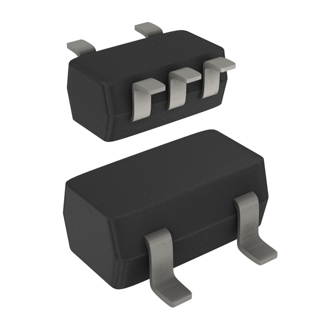
IC GATE AND 1CH 2-INP 5TSSOP
Datasheet:
Delivery:


Payment:


In Stock : 0
Please send RFQ , we will respond immediately.


74LVC1G08GW/DG,125 Specifications
-
TypeParameter
-
Package / Case5-TSSOP, SC-70-5, SOT-353
-
Supplier Device Package5-TSSOP
-
Mounting TypeSurface Mount
-
Operating Temperature-40°C ~ 125°C (TA)
-
Max Propagation Delay @ V, Max CL4ns @ 5V, 50pF
-
Input Logic Level - High1.7V ~ 2V
-
Input Logic Level - Low0.7V ~ 0.8V
-
Current - Output High, Low32mA, 32mA
-
Current - Quiescent (Max)200 µA
-
Voltage - Supply1.65V ~ 5.5V
-
Features-
-
Number of Inputs2
-
Number of Circuits1
-
Logic TypeAND Gate
-
PackagingTape & Reel (TR)
-
Product StatusObsolete
-
Series74LVC
The 74LVC1G08GW/DG,125 is a single 2-input AND gate chip belonging to the 74LVC series of integrated circuits. Some of its advantages and application scenarios are as follows:Advantages: 1. Wide operating voltage range: The chip can operate within a wide voltage range of 1.65V to 5.5V, making it suitable for various applications. 2. Low power consumption: The chip has low power dissipation, making it energy-efficient. 3. Fast switching speed: It has a high-speed operation of up to 5.8 ns propagation delay. 4. Compatibility: The chip is fully specified for partial power-down applications and is compatible with other 3.3V and 5V logic families.Application scenarios: 1. Logic gates: The 74LVC1G08GW/DG,125 chip can be used to implement different logic functions by connecting multiple gates together. For example, it can be combined with other gates to create complex logic circuits. 2. Data switching: The chip is suitable for data switching applications, where it can route or control the flow of data signals based on logic inputs. 3. Signal conditioning: It can be used in various signal conditioning circuits, such as level shifting or signal inversion applications. 4. Interface translation: The chip can be utilized to convert logic levels between different voltage domains, allowing communication between different devices or systems. 5. Battery-powered devices: Due to its low power consumption and wide operating voltage range, the chip is well-suited for battery-operated devices or portable electronics.Overall, the 74LVC1G08GW/DG,125 chip offers advantages like wide operating voltage range, low power consumption, and fast switching speed, making it versatile for various applications ranging from basic logic gates to signal conditioning and interface translation.
74LVC1G08GW/DG,125 Relevant information
