


Share

CD4009UBPWE4
Manufacturer No:
CD4009UBPWE4
Manufacturer:
Description:
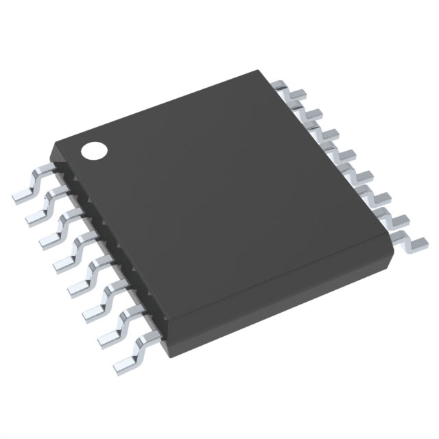
IC INVERTER 6CH 1-INP 16TSSOP
Datasheet:
Delivery:


Payment:


In Stock : 0
Please send RFQ , we will respond immediately.


CD4009UBPWE4 Specifications
-
TypeParameter
-
Package / Case16-TSSOP (0.173", 4.40mm Width)
-
Supplier Device Package16-TSSOP
-
Mounting TypeSurface Mount
-
Operating Temperature-55°C ~ 125°C
-
Max Propagation Delay @ V, Max CL60ns @ 15V, 50pF
-
Input Logic Level - High4V ~ 12.5V
-
Input Logic Level - Low1V ~ 2.5V
-
Current - Output High, Low1.5mA, 24mA
-
Current - Quiescent (Max)4 µA
-
Voltage - Supply3V ~ 18V
-
Features-
-
Number of Inputs1
-
Number of Circuits6
-
Logic TypeInverter
-
PackagingTube
-
Product StatusObsolete
-
Series4000B
The CD4009UBPWE4 is a CMOS hex inverter/buffer integrated circuit chip. It offers several advantages and can be used in various application scenarios:Advantages: 1. Low power consumption: The CD4009UBPWE4 operates at very low power levels, making it suitable for battery-powered devices and energy-efficient applications. 2. Wide supply voltage range: It can operate within a wide supply voltage range of 3V to 18V, providing flexibility in different power supply configurations. 3. High noise immunity: The chip has a high noise immunity, making it less susceptible to external noise and ensuring reliable operation in noisy environments. 4. High input impedance: The CD4009UBPWE4 has a high input impedance, allowing it to interface easily with different types of input signals. 5. High output current: It can provide a high output current, enabling it to drive capacitive loads and multiple devices without significant degradation in performance.Application scenarios: 1. Logic level conversion: The CD4009UBPWE4 can be used to convert logic levels between different voltage domains, allowing interfacing between devices operating at different voltage levels. 2. Signal buffering: It can be used to buffer and amplify weak signals, ensuring signal integrity and preventing signal degradation in long-distance transmission or noisy environments. 3. Oscillator circuits: The chip can be used to build oscillator circuits for generating clock signals or timing signals in various applications. 4. Waveform shaping: It can be used to shape and condition input waveforms, such as squaring up signals or removing noise from input signals. 5. Logic gates: The CD4009UBPWE4 can be used as a basic building block for implementing logic gates, such as inverters, buffers, and gate combinations, in digital circuits.Overall, the CD4009UBPWE4 offers low power consumption, wide supply voltage range, and high noise immunity, making it suitable for a range of applications requiring logic level conversion, signal buffering, waveform shaping, and basic logic gate implementation.
CD4009UBPWE4 Relevant information
