


Share

CD4009UBM96
Manufacturer No:
CD4009UBM96
Manufacturer:
Description:
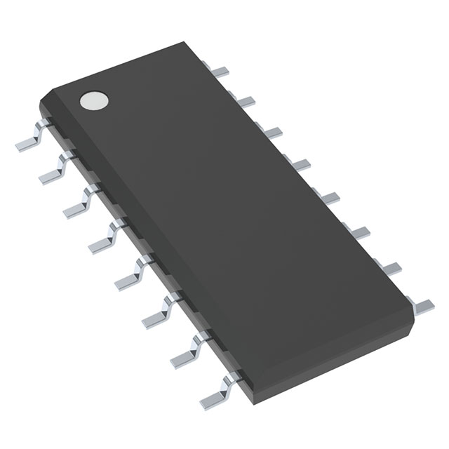
IC INVERTER 6CH 1-INP 16SOIC
Datasheet:
Delivery:


Payment:


In Stock : 0
Please send RFQ , we will respond immediately.


CD4009UBM96 Specifications
-
TypeParameter
-
Package / Case16-SOIC (0.154", 3.90mm Width)
-
Supplier Device Package16-SOIC
-
Mounting TypeSurface Mount
-
Operating Temperature-55°C ~ 125°C
-
Max Propagation Delay @ V, Max CL60ns @ 15V, 50pF
-
Input Logic Level - High4V ~ 12.5V
-
Input Logic Level - Low1V ~ 2.5V
-
Current - Output High, Low1.5mA, 24mA
-
Current - Quiescent (Max)4 µA
-
Voltage - Supply3V ~ 18V
-
Features-
-
Number of Inputs1
-
Number of Circuits6
-
Logic TypeInverter
-
PackagingTape & Reel (TR)
-
Product StatusObsolete
-
Series4000B
The CD4009UBM96 is a CMOS hex inverter/buffer integrated circuit chip. It offers several advantages and can be used in various application scenarios:Advantages: 1. Low power consumption: The CD4009UBM96 operates at very low power levels, making it suitable for battery-powered devices and applications where power efficiency is crucial. 2. Wide operating voltage range: It can operate within a wide voltage range, typically from 3V to 18V, making it compatible with a variety of power supply configurations. 3. High noise immunity: The chip has a high noise immunity, which means it can tolerate external noise and interference, ensuring reliable operation in noisy environments. 4. High input impedance: The CD4009UBM96 has a high input impedance, making it less sensitive to input signal variations and allowing it to interface easily with other circuits. 5. Compact and cost-effective: The chip is available in a small package, making it suitable for space-constrained applications. It is also cost-effective due to its integration of multiple inverters/buffers in a single chip.Application scenarios: 1. Logic level conversion: The CD4009UBM96 can be used to convert logic levels between different voltage domains, enabling communication between circuits operating at different voltage levels. 2. Signal buffering: It can be used to buffer and amplify weak signals, ensuring signal integrity and preventing signal degradation over long distances or when driving multiple loads. 3. Oscillator circuits: The chip can be used to build oscillator circuits for generating clock signals or timing signals in various digital systems. 4. Waveform shaping: It can be used to shape and condition input waveforms, such as squaring up signals or removing noise from input signals. 5. Logic gates: The CD4009UBM96 can be used to implement various logic functions, such as AND, OR, NAND, NOR, XOR, and XNOR gates, in digital circuits.Overall, the CD4009UBM96 offers versatility, low power consumption, and noise immunity, making it suitable for a wide range of applications in digital systems, communication devices, and other electronic circuits.
CD4009UBM96 Relevant information
