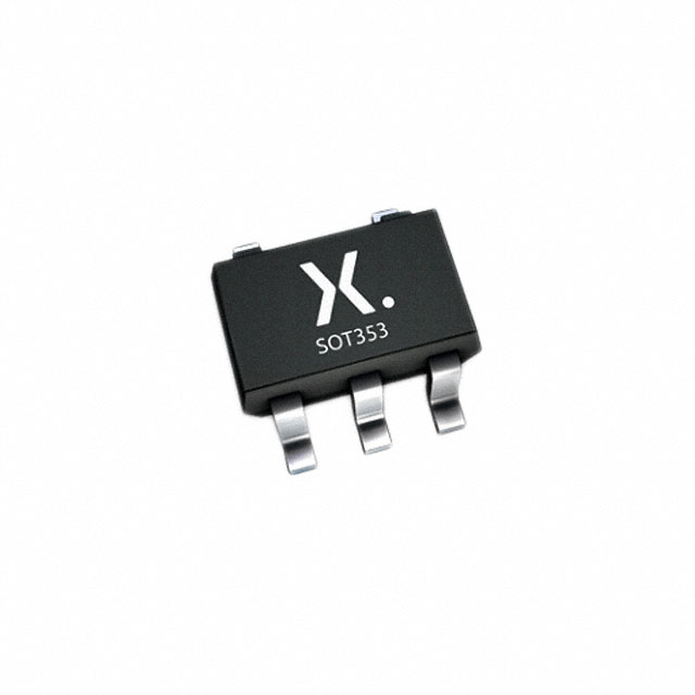
74LVC1G08GW,165
Manufacturer No:
74LVC1G08GW,165
Manufacturer:
Description:
IC GATE AND 1CH 2-INP 5TSSOP
Datasheet:
Delivery:


Payment:


In Stock : 0
Please send RFQ , we will respond immediately.


74LVC1G08GW,165 Specifications
-
TypeParameter
-
Package / Case5-TSSOP, SC-70-5, SOT-353
-
Supplier Device Package5-TSSOP
-
Mounting TypeSurface Mount
-
Operating Temperature-40°C ~ 125°C (TA)
-
Max Propagation Delay @ V, Max CL4ns @ 5V, 50pF
-
Input Logic Level - High1.7V ~ 2V
-
Input Logic Level - Low0.7V ~ 0.8V
-
Current - Output High, Low32mA, 32mA
-
Current - Quiescent (Max)4 µA
-
Voltage - Supply1.65V ~ 5.5V
-
Features-
-
Number of Inputs2
-
Number of Circuits1
-
Logic TypeAND Gate
-
PackagingTape & Reel (TR)
-
Product StatusObsolete
-
Series74LVC
The 74LVC1G08GW and 165 are both integrated circuit chips that serve different purposes and have different advantages and application scenarios.Advantages and Application Scenarios of 74LVC1G08GW: 1. Advantages: - Low voltage operation: The "LVC" in the name stands for Low Voltage CMOS, indicating that this chip operates at low voltage levels, typically around 1.8V to 5V. This makes it suitable for use in battery-powered devices or low-power applications. - High-speed operation: The "1G08" in the name refers to a 2-input AND gate, which means this chip can perform logical AND operations on two input signals. The "GW" indicates that it is a single-gate package. The 74LVC1G08GW is designed for high-speed operation, making it suitable for applications that require fast signal processing. - Small form factor: The chip is available in a small SOT353 package, which makes it suitable for space-constrained applications.2. Application Scenarios: - Logic gates: The 74LVC1G08GW is commonly used as a basic building block for logic gates in digital circuits. It can be used to implement AND gates, OR gates, XOR gates, etc. - Signal conditioning: It can be used for signal conditioning or level shifting in various applications, such as interfacing between different voltage domains or converting analog signals to digital signals. - Buffering: The chip can be used as a buffer to isolate or amplify signals in a circuit. - Clock distribution: It can be used for clock distribution in digital systems, ensuring that clock signals are properly propagated to different parts of the system.Advantages and Application Scenarios of 165: 1. Advantages: - Serial-to-parallel conversion: The 165 is a parallel-in, serial-out shift register, which means it can convert serial data input into parallel data output. This is useful in applications where data needs to be serialized or deserialized. - High-speed operation: The 165 is designed for high-speed operation, making it suitable for applications that require fast data transfer. - Multiple inputs: The chip has multiple parallel inputs, allowing it to handle multiple data inputs simultaneously.2. Application Scenarios: - Serial communication: The 165 can be used in serial communication protocols like SPI (Serial Peripheral Interface) or I2C (Inter-Integrated Circuit) to convert serial data into parallel data for further processing. - Data storage: It can be used for temporary data storage or data buffering in applications where data needs to be stored temporarily before being processed or transmitted. - Data acquisition: The 165 can be used in data acquisition systems to capture and process data from multiple sources simultaneously. - Shift register applications: It can be used in various applications that require serial-to-parallel conversion, such as LED displays, digital counters, or data multiplexing.
74LVC1G08GW,165 Relevant information


