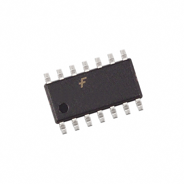
In Stock : 0
Please send RFQ , we will respond immediately.


CD4011BCSJ Specifications
-
TypeParameter
-
Current - Quiescent (Max)1 µA
-
Package / Case14-SOIC (0.209", 5.30mm Width)
-
Supplier Device Package14-SOP
-
Mounting TypeSurface Mount
-
Operating Temperature-55°C ~ 125°C
-
Max Propagation Delay @ V, Max CL70ns @ 15V, 50pF
-
Input Logic Level - High3.5V ~ 11V
-
Input Logic Level - Low1.5V ~ 4V
-
Current - Output High, Low3.4mA, 3.4mA
-
Voltage - Supply3V ~ 15V
-
Features-
-
Number of Inputs2
-
Number of Circuits4
-
Logic TypeNAND Gate
-
PackagingTube
-
Product StatusObsolete
-
Series4000B
The CD4011BCSJ is a specific integrated circuit chip that belongs to the CD4000 series of CMOS logic gates. It is a quad 2-input NAND gate chip, which means it contains four separate NAND gates, each with two inputs. Here are some advantages and application scenarios of the CD4011BCSJ chip:Advantages: 1. Low power consumption: The CD4011BCSJ chip operates at a low power supply voltage, making it suitable for battery-powered devices and energy-efficient applications. 2. Wide operating voltage range: It can operate within a wide range of power supply voltages, typically from 3V to 18V, providing flexibility in various electronic systems. 3. High noise immunity: The chip has a high noise immunity, which means it can tolerate external noise and interference, ensuring reliable operation in noisy environments. 4. Compact size: The CD4011BCSJ chip comes in a small package, making it suitable for space-constrained applications and integration into compact electronic devices.Application scenarios: 1. Digital logic circuits: The CD4011BCSJ chip can be used to implement various digital logic functions, such as AND, OR, and NOT gates. It is commonly used in digital systems for signal processing, data manipulation, and control. 2. Signal conditioning: It can be used for signal conditioning and level shifting in analog and digital circuits. For example, it can convert a high-level signal to a low-level signal or vice versa. 3. Oscillators and timers: The NAND gates in the CD4011BCSJ chip can be configured to build oscillators and timers for generating clock signals, time delays, and frequency generation. 4. Interface circuits: It can be used as an interface between different logic families or voltage levels, enabling compatibility between different parts of a system. 5. DIY electronics projects: The CD4011BCSJ chip is popular among hobbyists and electronics enthusiasts for building custom logic circuits, prototyping, and experimenting.Remember to consult the datasheet and relevant documentation for detailed specifications and guidelines when using the CD4011BCSJ chip in your specific application.
CD4011BCSJ Relevant information


