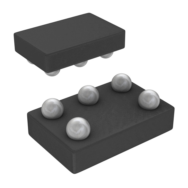
SN74LVC1G332YEPR
Manufacturer No:
SN74LVC1G332YEPR
Manufacturer:
Description:
IC GATE OR 1CH 3-INP 5DSBGA
Datasheet:
Delivery:


Payment:


In Stock : 0
Please send RFQ , we will respond immediately.


SN74LVC1G332YEPR Specifications
-
TypeParameter
-
Package / Case5-XFBGA, DSBGA
-
Supplier Device Package5-DSBGA (1.4x0.9)
-
Mounting TypeSurface Mount
-
Operating Temperature-40°C ~ 85°C
-
Max Propagation Delay @ V, Max CL3.5ns @ 5V, 50pF
-
Input Logic Level - High1.7V ~ 2V
-
Input Logic Level - Low0.7V ~ 0.8V
-
Current - Output High, Low32mA, 32mA
-
Current - Quiescent (Max)10 µA
-
Voltage - Supply1.65V ~ 5.5V
-
Features-
-
Number of Inputs3
-
Number of Circuits1
-
Logic TypeOR Gate
-
PackagingBulk
-
PackagingCut Tape (CT)
-
PackagingTape & Reel (TR)
-
Product StatusObsolete
-
Series74LVC
The SN74LVC1G332YEPR is a single-gate buffer/driver integrated circuit chip manufactured by Texas Instruments. It offers several advantages and can be used in various application scenarios. Some of the advantages and application scenarios of the SN74LVC1G332YEPR are:Advantages: 1. Small package size: The chip comes in a small SOT-23 package, making it suitable for space-constrained applications. 2. Low power consumption: It operates at low power supply voltages (1.65V to 5.5V) and consumes minimal power, making it ideal for battery-powered devices. 3. High-speed operation: The chip has a high-speed propagation delay of 3.8ns, enabling fast signal transmission. 4. Wide operating temperature range: It can operate in a temperature range of -40°C to 125°C, making it suitable for various environments. 5. ESD protection: The chip provides ESD protection up to 2kV, ensuring robustness against electrostatic discharge.Application Scenarios: 1. Signal buffering: The SN74LVC1G332YEPR can be used to buffer and amplify signals in various digital systems, ensuring proper signal integrity and driving capability. 2. Level shifting: It can be used to shift logic levels between different voltage domains, allowing compatibility between devices operating at different voltage levels. 3. Clock distribution: The chip can be used to distribute clock signals in synchronous digital systems, ensuring accurate and synchronized timing across multiple components. 4. I/O expansion: It can be used to expand the number of input/output pins of microcontrollers or other digital devices, enabling connectivity with a larger number of peripherals. 5. Voltage translation: The chip can be used to translate logic levels between different voltage standards, facilitating communication between devices with different voltage requirements.These are just a few examples of the advantages and application scenarios of the SN74LVC1G332YEPR. The chip's versatility, small size, low power consumption, and high-speed operation make it suitable for a wide range of digital applications.
SN74LVC1G332YEPR Relevant information


