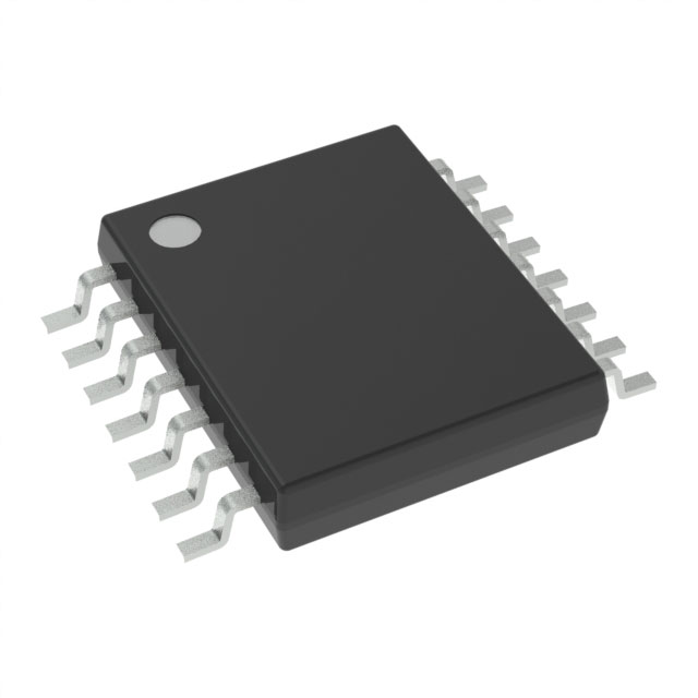
SN74LVC08APWRG3
Manufacturer No:
SN74LVC08APWRG3
Manufacturer:
Description:
IC GATE AND 4CH 2-INP 14TSSOP
Datasheet:
Delivery:


Payment:


In Stock : 6749
Please send RFQ , we will respond immediately.


SN74LVC08APWRG3 Specifications
-
TypeParameter
-
Package / Case14-TSSOP (0.173", 4.40mm Width)
-
Supplier Device Package14-TSSOP
-
Mounting TypeSurface Mount
-
Operating Temperature-40°C ~ 125°C
-
Max Propagation Delay @ V, Max CL3.9ns @ 3.3V, 50pF
-
Input Logic Level - High1.7V ~ 2V
-
Input Logic Level - Low0.7V ~ 0.8V
-
Current - Output High, Low24mA, 24mA
-
Current - Quiescent (Max)1 µA
-
Voltage - Supply1.65V ~ 3.6V
-
Features-
-
Number of Inputs2
-
Number of Circuits4
-
Logic TypeAND Gate
-
PackagingCut Tape (CT)
-
PackagingTape & Reel (TR)
-
Product StatusActive
-
Series74LVC
The SN74LVC08APWRG3 is a quad 2-input AND gate integrated circuit chip manufactured by Texas Instruments. It offers several advantages and can be used in various application scenarios. Here are some advantages and application scenarios of the SN74LVC08APWRG3:Advantages: 1. Low power consumption: The SN74LVC08APWRG3 operates at a low voltage, making it suitable for battery-powered devices and low-power applications. 2. High-speed operation: With a propagation delay of only 2.7 ns, this chip enables fast switching and efficient operation in high-speed digital circuits. 3. Wide supply voltage range: It can operate over a wide range of supply voltages, from 1.65V to 5.5V, making it versatile and compatible with various logic families. 4. 5V tolerant inputs: The chip has 5V tolerant inputs, allowing direct interfacing with other standard logic families, including TTL. 5. ESD protection: The SN74LVC08APWRG3 provides electrostatic discharge (ESD) protection, ensuring the device's robustness and reliability in demanding environments.Application scenarios: 1. Digital systems: It is commonly used in digital systems, such as microcontrollers, processors, and FPGA-based designs, to perform logical AND operations between input signals. 2. Signal conditioning: The AND gate functionality of this chip can be utilized for signal conditioning, where specific input signals need to be combined and processed to generate output signals based on certain conditions. 3. Serial data communication: It can be employed in serial data communication systems to perform logical operations on received data signals. 4. Memory control: The SN74LVC08APWRG3 can also be used in memory control circuits to facilitate data validation and control signals for read and write operations. 5. Interface circuits: Due to its 5V tolerant inputs, it can be useful in interfacing different logic families and voltage levels, bridging the gap between various signal levels.It is important to note that while these advantages and application scenarios are common, the specific implementation and use of the SN74LVC08APWRG3 can vary based on the requirements of the particular circuit or system.
SN74LVC08APWRG3 Relevant information


